
Datasheet


Table Of Contents
- 1 Features
- 2 Applications
- 3 Description
- 4 Simplified Schematic
- Table of Contents
- 5 Revision History
- 6 Pin Configuration and Functions
- 7 Specifications
- 8 Parameteric Measurement Information
- 9 Detailed Description
- 10 Application and Implementation
- 11 Power Supply Recommendations
- 12 Layout
- 13 Device and Documentation Support
- 14 Mechanical, Packaging, and Orderable Information
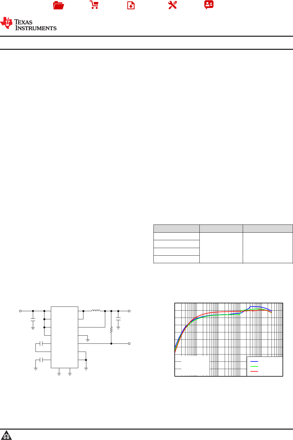
50
55
60
65
70
75
80
85
90
95
100
100m 1 10 100 1k 10k
I load (mA)
Efficiency (%)
V
IN
= 3.7 V
V
IN
= 4.2 V
V
IN
= 5 V
V
OUT
= 3.3 V
L = 1 µH
f = 1.4 MHz
G002
Vout
1.8V/3A
Vin
2.5V to 6V
PVIN
PVIN
EN FB
C1
10 Fm
L1
470nH
C2
22 Fm
SW
TPS62090
SW
Power Good
AVIN
SS
R3
500k
AGND
PG
C4
10nF
VOS
FREQ
CP
CN
C3
10nF
1
2
3
4
5
6
PGND PGND
7
8
9
10
11
12
13
14 15
16
Product
Folder
Sample &
Buy
Technical
Documents
Tools &
Software
Support &
Community
TPS62090
,
TPS62091
,
TPS62092
,
TPS62093
SLVSAW2B –MARCH 2012–REVISED APRIL 2014
TPS6209x 3A High Efficient Synchronous Step Down Converter with DCS ™ Control
1 Features 3 Description
The TPS6209x device family is a high frequency
1
• 2.5 V to 6 V Input Voltage Range
synchronous step down converter optimized for small
• DCS™ Control
solution size, high efficiency and suitable for battery
• 95% Converter Efficiency
powered applications. To maximize efficiency, the
converter operates in PWM mode with a nominal
• Power Save Mode
switching frequency of 2.8 MHz/1.4 MHz and
• 20 µA Operating Quiescent Current
automatically enters Power Save Mode operation at
• 100% Duty Cycle for Lowest Dropout
light load currents. When used in distributed power
supplies and point of load regulation, the device
• 2.8 MHz/1.4 MHz Typical Switching Frequency
allows voltage tracking to other voltage rails and
• 0.8 V to V
IN
Adjustable Output Voltage
tolerates output capacitors ranging from 10 µF up to
• Fixed Output Voltage Versions
150 µF and beyond. Using the DCS™ Control
• Output Discharge Function
topology the device achieves excellent load transient
performance and accurate output voltage regulation.
• Adjustable Softstart
• Two Level Short Circuit Protection
The output voltage start-up ramp is controlled by the
softstart pin, which allows operation as either a
• Output Voltage Tracking
standalone power supply or in tracking configurations.
• Wide Output Capacitance Selection
Power sequencing is also possible by configuring the
Enable and Power Good pins. In Power Save Mode,
2 Applications
the device operates at typically 20 µA quiescent
current. Power Save Mode is entered automatically
• Distributed Power Supplies
and seamlessly maintaining high efficiency over the
• Notebook, Netbook Computers
entire load current range.
• Hard Disk Drivers (HDD)
Device Information
(1)
• Solid State Drives (SSD)
DEVICE NAME PACKAGE BODY SIZE
• Processor Supply
TPS62090
• Battery Powered Applications
TPS62091
QFN (16) 3mm x 3mm
TPS62092
TPS62093
(1) For all available packages, see the orderable addendum at
the end of the data sheet.
4 Simplified Schematic
Efficiency vs Output Current
1
An IMPORTANT NOTICE at the end of this data sheet addresses availability, warranty, changes, use in safety-critical applications,
intellectual property matters and other important disclaimers. PRODUCTION DATA.