
Datasheet

TPS62110-Q1
www.ti.com
SLVSA54A –FEBRUARY 2010–REVISED SEPTEMBER 2012
17-V 1.5-A SYNCHRONOUS STEP-DOWN CONVERTER
Check for Samples: TPS62110-Q1
1
FEATURES
• Up to 1.5-A Output Current
• High Efficiency Over a Wide Load Current
• Qualified for Automotive Applications
Range Due to PFM/PWM Operation Mode
• AEC-Q100 Qualified With the Following
• 100% Maximum Duty Cycle for Lowest
Results:
Dropout
– Device Temperature Grade 1: –40°C to
• 20-µA Quiescent Current (Typical)
125°C Ambient Operating Temperature
Range
• Overtemperature and Overcurrent Protected
– Device HBM ESD Classification Level H2
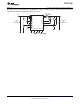
• Available in 16 Pin QFN Package
– Device CDM ESD Classification Level C3B
• High-Efficiency Synchronous Step-Down
Converter With up to 95% Efficiency
• 3.1-V to 17-V Operating Input Voltage Range
• Adjustable Output Voltage Range
From 1.2 V to 16 V
• Synchronizable to External Clock Signal up to
1.4 MHz
DESCRIPTION/ORDERING INFORMATION
The TPS62110 is a low-noise synchronous step-down dc-dc converter that is ideally suited for systems powered
from a 2-cell Li-ion battery or from a 12-V or 15-V rail.
The TPS62110 is a synchronous PWM converter with integrated N-channel and P-channel power MOSFET
switches. Synchronous rectification is used to increase efficiency and to reduce external component count. To
achieve highest efficiency over a wide load current range, the converter enters a power-saving, pulse-frequency
modulation (PFM) mode at light load currents. Operating frequency is typically 1 MHz, allowing the use of small
inductor and capacitor values. The device can be synchronized to an external clock signal in the range of 0.8
MHz to 1.4 MHz. For low noise operation, the converter can be operated in PWM-only mode. In the shutdown
mode, the current consumption is reduced to less than 2 µA. The TPS62110 is available in the 16-pin (RSA)
QFN package and operates over a free-air temperature range of –40°C to 125°C.
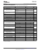
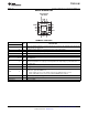
ORDERING INFORMATION
(1)(2)
T
A
ORDERABLE PART NUMBER TOP-SIDE MARKING
–40°C to 125°C TPS62110QRSARQ1 TPS62110Q
(1) For the most current package and ordering information, see the Package Option Addendum at the end of this document, or see the TI
web site at www.ti.com.
(2) Package drawings, thermal data, and symbolization are available at www.ti.com/packaging.
1
Please be aware that an important notice concerning availability, standard warranty, and use in critical applications of
Texas Instruments semiconductor products and disclaimers thereto appears at the end of this data sheet.
PRODUCTION DATA information is current as of publication date.
Copyright © 2010–2012, Texas Instruments Incorporated
Products conform to specifications per the terms of the Texas
Instruments standard warranty. Production processing does not
necessarily include testing of all parameters.