
Datasheet
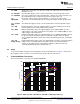

40
50
60
70
80
90
100
0.0001 0.001 0.01 0.1 1 10
Load Current - A
V = 5 V
I
V = 9 V
I
V = 12 V
I
V = 15 V
I
V = 17 V
I
Efficiency - %
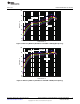
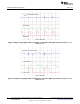
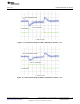
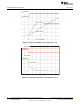
TPS621x0EVM-505 Test Results
www.ti.com
J6 – GND Output return connection. Use when the steady-state output current is less than 1 A.
Otherwise, use J9.
J7 – PG/GND The PG output appears on pin 1 of this header with a convenient ground on pin 2.
J8 – VIN/GND Pin 1 is the positive input connection with pin 2, serving as the return connection. Use
this terminal block if the steady-state input current is greater than 1 A.
J9 – Pin 2 is the output voltage connection with pin 1, serving as the output return
VOUT/GND connection. Use this terminal block if the steady-state output current is greater than 1
A.
J10 – SS/TR & The SS/TR input appears on pin 1 of this header with a convenient ground on pin 2
GND
JP1 – EN EN pin input jumper. Place the supplied jumper across ON and EN to turn on the IC.
Place the jumper across OFF and EN to turn off the IC.
JP2 – DEF DEF pin input jumper. Place the supplied jumper across HIGH and DEF to set the
output voltage at 5% above nominal. Place the jumper across LOW and DEF to set the
output voltage at the nominal level.
JP3 – FSW FSW pin input jumper. Place the supplied jumper across 1.25MHz and FSW to operate
the IC at a reduced switching frequency of nominally 1.25 MHz. Place the jumper
across 2.5MHz and FSW to operate the IC at the full switching frequency of nominally
2.5 MHz.
JP4 – PG PG pin pullup voltage jumper. Place the supplied jumper on JP4 to connect the PG pin
Pullup Voltage pullup resistor to Vout. Alternatively, the jumper can be removed and a different
voltage can be supplied on pin 2 to pull up the PG pin to a different level. This
externally applied voltage must remain below 7 V.
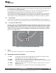
2.2 Setup
To operate the EVM, set jumpers JP1 through JP4 to the desired positions per Section 2.1. Connect the
input supply to either J1 and J3 or J8, and connect the load to either J4 and J6 or J9.
3 TPS621x0EVM-505 Test Results
This section provides test results of the TPS621x0EVM-505.
Figure 2. Efficiency With 1-µH Inductor and FSW = LOW (high frequency)
4
TPS62130EVM-505, TPS62140EVM-505, and TPS62150EVM-505 SLVU437A–October 2011–Revised July 2013
Evaluation Modules
Submit Documentation Feedback
Copyright © 2011–2013, Texas Instruments Incorporated