
Datasheet


www.ti.com
3
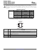
2
4
5
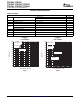
DBV PACKAGE
(TOP VIEW)
1
V
I
GND
EN
SW
FB
TPS62200 , , TPS62201
TPS62202 , TPS62203 , TPS62207
TPS62204 , TPS62205 , TPS62208
SLVS417E – MARCH 2002 – REVISED MAY 2006
This integrated circuit can be damaged by ESD. Texas Instruments recommends that all integrated circuits be handled with
appropriate precautions. Failure to observe proper handling and installation procedures can cause damage.
ESD damage can range from subtle performance degradation to complete device failure. Precision integrated circuits may be
more susceptible to damage because very small parametric changes could cause the device not to meet its published
specifications.
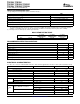
ORDERING INFORMATION
(1)
T
A
OUTPUT VOLTAGE SOT23 PACKAGE SYMBOL
Adjustable TPS62200DBV PHKI
1.2 V TPS62207DBV PJGI
1.5 V TPS62201DBV PHLI
1.6 V TPS62204DBV PHSI
-40°C to 85°C
1.8 V TPS62202DBV PHMI
1.875 V TPS62208DBV ALW
2.5 V TPS62205DBV PHTI
3.3 V TPS62203DBV PHNI
(1) The DBV package is available in tape and reel. Add R suffix (DBVR) to order quantities of 3000 parts.
Add T suffix (DBVT) to order quantities of 250 parts
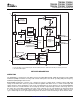
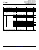
Terminal Functions
TERMINAL
I/O DESCRIPTION
NAME NO.
This is the enable pin of the device. Pulling this pin to ground forces the device into shutdown mode. Pulling this
EN 3 I
pin to Vin enables the device. This pin must not be left floating and must be terminated.
This is the feedback pin of the device. Connect this pin directly to the output if the fixed output voltage version is
FB 4 I used. For the adjustable version an external resistor divider is connected to this pin. The internal voltage divider
is disabled for the adjustable version.
GND 2 Ground
SW 5 I/O Connect the inductor to this pin. This pin is the switch pin and is connected to the internal MOSFET switches.
V
I
1 I Supply voltage pin
2
Submit Documentation Feedback