
Datasheet


www.ti.com
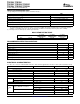
ABSOLUTE MAXIMUM RATINGS
DISSIPATION RATING TABLE
RECOMMENDED OPERATING CONDITIONS
ELECTRICAL CHARACTERISTICS
TPS62200 , , TPS62201
TPS62202 , TPS62203 , TPS62207
TPS62204 , TPS62205 , TPS62208
SLVS417E – MARCH 2002 – REVISED MAY 2006
over operating free-air temperature (unless otherwise noted)
(1)
UNIT
Supply voltages, V
I
(2)
-0.3 V to 7.0 V
Voltages on pins SW, EN, FB
(2)
-0.3 V to V
CC
+0.3 V
Continuous power dissipation, P
D
See Dissipation Rating Table
Operating junction temperature range, T
J
-40°C to 150°C
Storage temperature, T
stg
-65°C to 150°C
Lead temperature (soldering, 10 sec) 260°C
(1) Stresses beyond those listed under "absolute maximum ratings" may cause permanent damage to the device. These are stress ratings
only, and functional operation of the device at these or any other conditions beyond those indicated under "recommended operating
conditions" is not implied. Exposure to absolute-maximum-rated conditions for extended periods may affect device reliability.
(2) All voltage values are with respect to network ground terminal.
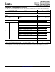
T
A
≤ 25°C T
A
= 70°C T
A
= 85°C
PACKAGE R
θ JA
POWER RATING POWER RATING POWER RATING
DBV 250°/W 400 mW 220 mW 160 mW
MIN NOM MAX UNIT
Supply voltage, V
I
2.5 6.0 V
Output voltage range for adjustable output voltage version, V
O
0.7 V
I
V
Output current, I
O
300 mA
Inductor, L
(1)
4.7 10 µH
Input capacitor, C
I
(1)
4.7 µF
Output capacitor, C
O
(1)
10 µF
Operating ambient temperature, T
A
40 85 °C
Operating junction temperature, T
J
40 125 °C
(1) See the application section for further information.
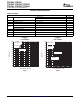
V
I
= 3.6 V, V
O
= 1.8 V, I
O
= 200 mA, EN = VIN, T
A
= -40 °C to 85 °C, typical values are at T
A
= 25 °C (unless otherwise noted)
PARAMETER TEST CONDITIONS MIN TYP MAX UNIT
SUPPLY CURRENT
V
I
Input voltage range 2.5 6.0 V
I
Q
Operating quiescent current I
O
= 0 mA, Device is not switching 15 30 µA
Shutdown supply current EN = GND 0.1 1 µA
Undervoltage lockout threshold 1.5 2.0 V
ENABLE
V
(EN)
EN high level input voltage 1.3 V
EN low level input voltage 0.4 V
I
(EN)
EN input bias current EN = GND or VIN 0.01 0.1 µA
POWER SWITCH
V
IN
= V
GS
= 3.6 V 530 690
P-channel MOSFET on-resistance m Ω
V
IN
= V
GS
= 2.5 V 670 850
r
ds
(ON)
V
IN
= V
GS
= 3.6 V 430 540
N-channel MOSFET on-resistance m Ω
V
IN
= V
GS
= 2.5 V 530 660
I
lkg_(P)
P-channel leakage current V
DS
= 6.0 V 0.1 1 µA
6
Submit Documentation Feedback