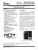
TPS62300, TPS62301, TPS62302 TPS62303, TPS62304, TPS62305, TPS62311, TPS62313, TPS62315, TPS62320, TPS62321 QFN-10 www.ti.com CSP-8 SLVS528E – JULY 2004 – REVISED NOVEMBER 2007 500-mA, 3-MHz SYNCHRONOUS STEP-DOWN CONVERTER IN CHIP SCALE PACKAGING FEATURES 1 • • • • • • • • Up to 93% Efficiency at 3-MHz Operation Up to 500-mA Output Current at VI = 2.7 V 3-MHz Fixed Frequency Operation Best in Class Load and Line Transient Complete 1-mm Component Profile Solution -0.5% / +1.
TPS62300, TPS62301, TPS62302 TPS62303, TPS62304, TPS62305, TPS62311, TPS62313, TPS62315, TPS62320, TPS62321 www.ti.com SLVS528E – JULY 2004 – REVISED NOVEMBER 2007 These devices have limited built-in ESD protection. The leads should be shorted together or the device placed in conductive foam during storage or handling to prevent electrostatic damage to the MOS gates.
TPS62300, TPS62301, TPS62302 TPS62303, TPS62304, TPS62305, TPS62311, TPS62313, TPS62315, TPS62320, TPS62321 www.ti.com SLVS528E – JULY 2004 – REVISED NOVEMBER 2007 ABSOLUTE MAXIMUM RATINGS over operating free-air temperature range (unless otherwise noted) (1) UNIT Voltage at VIN, AVIN (2) Voltage at SW VI -0.3 V to 7 V (2) -0.3 V to 7 V Voltage at FB, ADJ Voltage at EN, MODE/SYNC -0.3 V to 3.
TPS62300, TPS62301, TPS62302 TPS62303, TPS62304, TPS62305, TPS62311, TPS62313, TPS62315, TPS62320, TPS62321 www.ti.com SLVS528E – JULY 2004 – REVISED NOVEMBER 2007 DISSIPATION RATINGS (1) RθJA (2) POWER RATING FOR TA≤ 25°C DERATING FACTOR ABOVE TA = 25°C DRC 49°C/W 2050 mW 21 mW/°C YZD 250°C/W 400 mW 4 mW/°C YED 250°C/W 400 mW 4 mW/°C YZ 250°C/W 400 mW 4 mW/°C PACKAGE (1) (2) Maximum power dissipation is a function of TJ(max), θJA and TA.
TPS62300, TPS62301, TPS62302 TPS62303, TPS62304, TPS62305, TPS62311, TPS62313, TPS62315, TPS62320, TPS62321 www.ti.com SLVS528E – JULY 2004 – REVISED NOVEMBER 2007 ELECTRICAL CHARACTERISTICS (continued) VI = 3.6 V, VO = 1.6 V, EN = VI, MODE/SYNC = GND, L = 1 µH, CO = 10 µF, TA = -40°C to 85°C, typical values are at TA = 25°C (unless otherwise noted) PARAMETER TEST CONDITIONS MIN TYP MAX UNIT 3 OSCILLATOR fSW Oscillator frequency 2.65 3.35 MHz f(SYNC) Synchronization range 2.65 3.
TPS62300, TPS62301, TPS62302 TPS62303, TPS62304, TPS62305, TPS62311, TPS62313, TPS62315, TPS62320, TPS62321 www.ti.
TPS62300, TPS62301, TPS62302 TPS62303, TPS62304, TPS62305, TPS62311, TPS62313, TPS62315, TPS62320, TPS62321 www.ti.com SLVS528E – JULY 2004 – REVISED NOVEMBER 2007 FUNCTIONAL BLOCK DIAGRAM MODE/SYNC EN VIN N-MOS Current Limit Compator Undervoltage Lockout Bias Supply AVIN _ Soft-Start VREF = 0.
TPS62300, TPS62301, TPS62302 TPS62303, TPS62304, TPS62305, TPS62311, TPS62313, TPS62315, TPS62320, TPS62321 www.ti.
TPS62300, TPS62301, TPS62302 TPS62303, TPS62304, TPS62305, TPS62311, TPS62313, TPS62315, TPS62320, TPS62321 www.ti.com SLVS528E – JULY 2004 – REVISED NOVEMBER 2007 EFFICIENCY vs LOAD CURRENT EFFICIENCY vs LOAD CURRENT 100 90 PFM/PWM Operation L = 2.2 mH 80 90 80 70 60 Efficiency − % Efficiency − % 70 PWM Operation L = 2.2 mH 50 40 30 60 PWM Operation L = 0.9 mH 50 40 30 20 20 VI = 3.6 V, VO = 1.2 V 10 0 PFM/PWM Operation L = 2.2 mH 0.
TPS62300, TPS62301, TPS62302 TPS62303, TPS62304, TPS62305, TPS62311, TPS62313, TPS62315, TPS62320, TPS62321 www.ti.com SLVS528E – JULY 2004 – REVISED NOVEMBER 2007 IO = 10 to 400 mA Load Step MODE/SYNC = HIGH L = 0.9 mH, CO = 10 mF IO = 10 to 100 mA Load Step IO = 10 to 400 mA Load Step t − Time − 2 ms/div t − Time − 50 ms/div Figure 9. Figure 10. MODE/SYNC = HIGH L = 0.9 mH, CO = 10 mF IO = 400 to 10 mA Load Step IO = 100 to 10 mA Load Step t - Time - 2 ms/div Figure 11.
TPS62300, TPS62301, TPS62302 TPS62303, TPS62304, TPS62305, TPS62311, TPS62313, TPS62315, TPS62320, TPS62321 www.ti.com SLVS528E – JULY 2004 – REVISED NOVEMBER 2007 IO = 10 to 400 mA Load Step MODE/SYNC = HIGH L = 0.9 mH, CO = 4.7 mF IO = 10 to 100 mA Load Step IO = 10 to 400 mA Load Step t - Time - 2 ms/div t - Time - 50 ms/div Figure 13. Figure 14. MODE/SYNC = HIGH L = 0.9 mH, CO = 4.7 mF IO = 400 to 10 mA Load Step IO = 100 to 10 mA Load Step t - Time - 2 ms/div Figure 15.
TPS62300, TPS62301, TPS62302 TPS62303, TPS62304, TPS62305, TPS62311, TPS62313, TPS62315, TPS62320, TPS62321 www.ti.com SLVS528E – JULY 2004 – REVISED NOVEMBER 2007 OUTPUT VOLTAGE vs LOAD CURRENT 1.628 REGULATED FEEDBACK VOLTAGE vs TEMPERATURE 406 VI = 3.6 V, VO = 1.6 V, L = 2.2 mH V(FB) - Regulated Feedback Voltage - mV TPS62300 VO − Output Voltage − V 1.618 1.608 PWM Operation 1.598 1.588 PFM/PWM Operation 1.578 1 10 100 IO − Load Current − mA 404.5 404 403.5 403 VI = 2.7 V 402.
TPS62300, TPS62301, TPS62302 TPS62303, TPS62304, TPS62305, TPS62311, TPS62313, TPS62315, TPS62320, TPS62321 www.ti.com SLVS528E – JULY 2004 – REVISED NOVEMBER 2007 P-CHANNEL rDS(ON) vs INPUT VOLTAGE DUTY CYCLE JITTER 700 IO = 320 mA SW - 1 V/div TRIGGER ON RISING EDGE rDS(on) − Static Drain-Source On-Resistance − m Ω VI = 3.6 V, VO = 1.6 V, L = 0.9 mH, CO = 10 mF MODE/SYNC = HIGH TA = 855C 550 500 TA = 255C 450 400 350 300 TA = −405C 250 200 150 2.5 3 3.5 4 4.
TPS62300, TPS62301, TPS62302 TPS62303, TPS62304, TPS62305, TPS62311, TPS62313, TPS62315, TPS62320, TPS62321 www.ti.com SLVS528E – JULY 2004 – REVISED NOVEMBER 2007 DYNAMIC VOLTAGE MANAGEMENT L = 0.9 mH, CO = 10 mF IO = 40 mA V(ADJ) = 1 V L = 0.9 mH, CO = 10 mF, MODE/SYNC = LOW RL = 270 W t − Time − 20 ms/div DYNAMIC VOLTAGE MANAGEMENT START-UP VO = 1.5 V VI = 3.6 V, VO = 1.6 V, IO = 0 mA VO − 1 V/div VI = 3.6 V, VO = 1 V / 1.5 V EN − 2 V/div Figure 26. RL = 5 W L = 0.
TPS62300, TPS62301, TPS62302 TPS62303, TPS62304, TPS62305, TPS62311, TPS62313, TPS62315, TPS62320, TPS62321 www.ti.com SLVS528E – JULY 2004 – REVISED NOVEMBER 2007 POWER DOWN (TPS62321) L = 2.2 mH, CO = 4.7 mF, EN − 2 V/div VI = 3.6 V, VO = 1.5 V, IO = 0 mA VO − 500 mV/div V(ADJ) − 2 V/div VO − 1 V/div VI = 3.6 V, VO = 1.6 V, IO = 320 mA I L − 200 mA/div EN − 2 V/div START-UP L = 0.9 mH, CO = 10 mF t − Time − 400 ms/div t − Time − 50 ms/div Figure 29. Figure 30.
TPS62300, TPS62301, TPS62302 TPS62303, TPS62304, TPS62305, TPS62311, TPS62313, TPS62315, TPS62320, TPS62321 www.ti.com SLVS528E – JULY 2004 – REVISED NOVEMBER 2007 POWER-SAVE MODE With decreasing load current, the device automatically switches into pulse skipping operation in which the power stage operates intermittently based on load demand. By running cycles periodically, the switching losses are minimized, and the device runs with a minimum quiescent current and maintaining high efficiency.
www.ti.com TPS62300, TPS62301, TPS62302 TPS62303, TPS62304, TPS62305, TPS62311, TPS62313, TPS62315, TPS62320, TPS62321 SLVS528E – JULY 2004 – REVISED NOVEMBER 2007 LOW-DROPOUT OPERATION 100% DUTY CYCLE In 100% duty cycle mode, the TPS6230x, TPS6231x, and TPS6232x offer a low input-to-output voltage difference. In this mode, the P-channel MOSFET is constantly turned on.
TPS62300, TPS62301, TPS62302 TPS62303, TPS62304, TPS62305, TPS62311, TPS62313, TPS62315, TPS62320, TPS62321 www.ti.com SLVS528E – JULY 2004 – REVISED NOVEMBER 2007 APPLICATION INFORMATION ADJUSTABLE OUTPUT VOLTAGE When the adjustable output voltage versions, TPS62300 or TPS62320, are used, the output voltage is set by the external resistor divider (see Figure 32). The output voltage is calculated as: V O + 1.5 V ǒ1 ) R1 Ǔ with an internal reference voltage Vref typical + 0.
TPS62300, TPS62301, TPS62302 TPS62303, TPS62304, TPS62305, TPS62311, TPS62313, TPS62315, TPS62320, TPS62321 www.ti.com SLVS528E – JULY 2004 – REVISED NOVEMBER 2007 INDUCTOR SELECTION Even though the inductor does not influence the operating frequency, the inductor value has a direct effect on the ripple current. The selected inductor has to be rated for its dc resistance and saturation current. The inductor ripple current (ΔIL) decreases with higher inductance and increases with higher VI or VO.
TPS62300, TPS62301, TPS62302 TPS62303, TPS62304, TPS62305, TPS62311, TPS62313, TPS62315, TPS62320, TPS62321 www.ti.com SLVS528E – JULY 2004 – REVISED NOVEMBER 2007 INPUT CAPACITOR SELECTION Because of the nature of the buck converter having a pulsating input current, a low ESR input capacitor is required to prevent large voltage transients that can cause misbehavior of the device or interferences with other circuits in the system. For most applications, a 2.2-µF or 4.7-µF capacitor is sufficient.
TPS62300, TPS62301, TPS62302 TPS62303, TPS62304, TPS62305, TPS62311, TPS62313, TPS62315, TPS62320, TPS62321 www.ti.com SLVS528E – JULY 2004 – REVISED NOVEMBER 2007 LAYOUT CONSIDERATIONS As for all switching power supplies, the layout is an important step in the design. High-speed operation of the TPS6230x, TPS6231x, and TPS6232x devices demand careful attention to PCB layout. Care must be taken in board layout to get the specified performance.
TPS62300, TPS62301, TPS62302 TPS62303, TPS62304, TPS62305, TPS62311, TPS62313, TPS62315, TPS62320, TPS62321 www.ti.com SLVS528E – JULY 2004 – REVISED NOVEMBER 2007 THERMAL INFORMATION Implementation of integrated circuits in low-profile and fine-pitch surface-mount packages typically requires special attention to power dissipation.
TPS62300, TPS62301, TPS62302 TPS62303, TPS62304, TPS62305, TPS62311, TPS62313, TPS62315, TPS62320, TPS62321 www.ti.com SLVS528E – JULY 2004 – REVISED NOVEMBER 2007 APPLICATION EXAMPLES TPS62303YZD A2 2.7 V − 6 V C V IN B2 IN 10 µF C1 A1 VIN VOUT EN SW MODE/SYNC ADJ FB GND D1 L1 B1 V OUT C C2 1 Ch1 Ch2 1.
TPS62300, TPS62301, TPS62302 TPS62303, TPS62304, TPS62305, TPS62311, TPS62313, TPS62315, TPS62320, TPS62321 www.ti.com SLVS528E – JULY 2004 – REVISED NOVEMBER 2007 TPS62300 VIN VIN 1.8 VOUT L1 CI EN 10 µF SW R1 MODE/SYNC 2.2 µH ADJ 9.5 kΩ GND 2.85 V FB R2 8.2 kΩ DAC6571 VDD I2C I/F SDA SCL VDAC 1.6 VOUT C1 4.7 µF V O− Output Voltage − V 2.7 V − 6 V Default Voltage = R1 1.5 x Vref x 1+ R2 ( ) 1.4 1.2 1 0.8 0.6 0.4 DAC Control Range VO = 1.5 x 0.98 x V(DAC) 0.2 A0 GND 0 0 0.2 0.
PACKAGE OPTION ADDENDUM www.ti.
PACKAGE OPTION ADDENDUM www.ti.
PACKAGE OPTION ADDENDUM www.ti.
PACKAGE MATERIALS INFORMATION www.ti.com 22-Jan-2014 TAPE AND REEL INFORMATION *All dimensions are nominal Device Package Package Pins Type Drawing SPQ Reel Reel A0 Diameter Width (mm) (mm) W1 (mm) B0 (mm) K0 (mm) P1 (mm) W Pin1 (mm) Quadrant TPS62300DRCR SON DRC 10 3000 330.0 12.4 3.3 3.3 1.1 8.0 12.0 Q2 TPS62300YZDR DSBGA YZD 8 3000 180.0 8.4 1.11 2.11 0.81 4.0 8.0 Q1 TPS62300YZDT DSBGA YZD 8 250 180.0 8.4 1.11 2.11 0.81 4.0 8.
PACKAGE MATERIALS INFORMATION www.ti.com 22-Jan-2014 Device Package Package Pins Type Drawing SPQ Reel Reel A0 Diameter Width (mm) (mm) W1 (mm) B0 (mm) K0 (mm) P1 (mm) W Pin1 (mm) Quadrant TPS62311YZDT DSBGA YZD 8 250 180.0 8.4 1.11 2.11 0.81 4.0 8.0 Q1 TPS62313YZDR DSBGA YZD 8 3000 180.0 8.4 1.11 2.11 0.81 4.0 8.0 Q1 TPS62313YZDT DSBGA YZD 8 250 180.0 8.4 1.11 2.11 0.81 4.0 8.0 Q1 TPS62315YZR DSBGA YZ 8 3000 180.0 8.4 1.11 2.11 0.81 4.0 8.
PACKAGE MATERIALS INFORMATION www.ti.com 22-Jan-2014 Device Package Type Package Drawing Pins SPQ Length (mm) Width (mm) Height (mm) TPS62303YZDR DSBGA YZD 8 3000 220.0 220.0 34.0 TPS62303YZDT DSBGA YZD 8 250 220.0 220.0 34.0 TPS62304DRCR SON DRC 10 3000 338.1 338.1 20.6 TPS62304YZDR DSBGA YZD 8 3000 220.0 220.0 34.0 TPS62304YZDT DSBGA YZD 8 250 220.0 220.0 34.0 TPS62305DRCR SON DRC 10 3000 338.1 338.1 20.6 TPS62305YZDR DSBGA YZD 8 3000 220.
IMPORTANT NOTICE Texas Instruments Incorporated and its subsidiaries (TI) reserve the right to make corrections, enhancements, improvements and other changes to its semiconductor products and services per JESD46, latest issue, and to discontinue any product or service per JESD48, latest issue. Buyers should obtain the latest relevant information before placing orders and should verify that such information is current and complete.