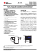
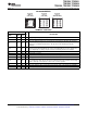
QFN-10 TPS62350, TPS62351 TPS62352, TPS62353 TPS62354, TPS62355, TPS62356 CSP-12 www.ti.com ..............................................................................................................................................................
TPS62350, TPS62351 TPS62352, TPS62353 TPS62354, TPS62355, TPS62356 SLVS540E – MAY 2006 – REVISED APRIL 2008 .............................................................................................................................................................. www.ti.com These devices have limited built-in ESD protection. The leads should be shorted together or the device placed in conductive foam during storage or handling to prevent electrostatic damage to the MOS gates.
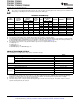
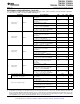
TPS62350, TPS62351 TPS62352, TPS62353 TPS62354, TPS62355, TPS62356 www.ti.com .............................................................................................................................................................. SLVS540E – MAY 2006 – REVISED APRIL 2008 RECOMMENDED OPERATING CONDITIONS over operating free-air temperature range (unless otherwise noted) MIN NOM MAX UNIT VI Input voltage range 2.7 5.
TPS62350, TPS62351 TPS62352, TPS62353 TPS62354, TPS62355, TPS62356 SLVS540E – MAY 2006 – REVISED APRIL 2008 .............................................................................................................................................................. www.ti.com ELECTRICAL CHARACTERISTICS (continued) over operating free-air temperature range, typical values are at TA = 25°C. Unless otherwise noted, specifications apply with VI = 3.6 V, EN = VI, VSEL = VI, SYNC = GND, VSEL0[6] bit = 1.
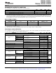
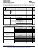
TPS62350, TPS62351 TPS62352, TPS62353 TPS62354, TPS62355, TPS62356 www.ti.com .............................................................................................................................................................. SLVS540E – MAY 2006 – REVISED APRIL 2008 ELECTRICAL CHARACTERISTICS (continued) over operating free-air temperature range, typical values are at TA = 25°C. Unless otherwise noted, specifications apply with VI = 3.6 V, EN = VI, VSEL = VI, SYNC = GND, VSEL0[6] bit = 1.
TPS62350, TPS62351 TPS62352, TPS62353 TPS62354, TPS62355, TPS62356 SLVS540E – MAY 2006 – REVISED APRIL 2008 .............................................................................................................................................................. www.ti.com ELECTRICAL CHARACTERISTICS (continued) over operating free-air temperature range, typical values are at TA = 25°C. Unless otherwise noted, specifications apply with VI = 3.6 V, EN = VI, VSEL = VI, SYNC = GND, VSEL0[6] bit = 1.
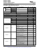
TPS62350, TPS62351 TPS62352, TPS62353 TPS62354, TPS62355, TPS62356 www.ti.com .............................................................................................................................................................. SLVS540E – MAY 2006 – REVISED APRIL 2008 I2C INTERFACE TIMING CHARACTERISTICS (continued) PARAMETER tSU, tSTA Setup Time for a Repeated START Condition tSU, tDAT Data Setup Time tHD, tDAT Data Hold Time TEST CONDITIONS MIN Standard mode 4.
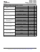
TPS62350, TPS62351 TPS62352, TPS62353 TPS62354, TPS62355, TPS62356 SLVS540E – MAY 2006 – REVISED APRIL 2008 .............................................................................................................................................................. www.ti.com I2C TIMING DIAGRAMS SDA tf tLOW tsu;DAT tr tf tBUF tr thd;STA SCL S thd;STA thd;DAT tsu;STA tsu;STO HIGH Sr P S Figure 1.
TPS62350, TPS62351 TPS62352, TPS62353 TPS62354, TPS62355, TPS62356 www.ti.com ..............................................................................................................................................................
TPS62350, TPS62351 TPS62352, TPS62353 TPS62354, TPS62355, TPS62356 SLVS540E – MAY 2006 – REVISED APRIL 2008 .............................................................................................................................................................. www.ti.
TPS62350, TPS62351 TPS62352, TPS62353 TPS62354, TPS62355, TPS62356 www.ti.com ..............................................................................................................................................................
TPS62350, TPS62351 TPS62352, TPS62353 TPS62354, TPS62355, TPS62356 SLVS540E – MAY 2006 – REVISED APRIL 2008 .............................................................................................................................................................. www.ti.com EFFICIENCY vs OUTPUT CURRENT EFFICIENCY vs OUTPUT CURRENT 100 100 90 90 VI = 3.6 V VO = 1.
TPS62350, TPS62351 TPS62352, TPS62353 TPS62354, TPS62355, TPS62356 www.ti.com .............................................................................................................................................................. SLVS540E – MAY 2006 – REVISED APRIL 2008 DC OUTPUT VOLTAGE vs OUTPUT CURRENT DC OUTPUT VOLTAGE vs INPUT VOLTAGE 1.070 0.790 0.785 1.065 0.780 1.060 VO − DC Output Voltage − V VO − DC Output Voltage − V LPFM/PWM Mode 1.055 PWM Mode 1.050 1.045 1.040 VO = 0.
TPS62350, TPS62351 TPS62352, TPS62353 TPS62354, TPS62355, TPS62356 SLVS540E – MAY 2006 – REVISED APRIL 2008 .............................................................................................................................................................. www.ti.com DC OUTPUT VOLTAGE vs AMBIENT TEMPERATURE MEASURED OUTPUT VOLTAGE vs DAC TARGET OUTPUT VOLTAGE 5 1.360 IO = 100 mA 4 L = 1 mH CO = 10 mF 3-MHz PWM Mode VO − Measured Output Voltage − mV VO − DC Output Voltage − V 1.
TPS62350, TPS62351 TPS62352, TPS62353 TPS62354, TPS62355, TPS62356 www.ti.com .............................................................................................................................................................. SLVS540E – MAY 2006 – REVISED APRIL 2008 OSCILLATOR FREQUENCY vs INPUT VOLTAGE rDS(on) P-MOSFET vs INPUT VOLTAGE 3.15 450 o 400 3.1 TA = 25 C 3.05 3 o TA = 85 C o TA = 85oC 2.95 rDS(on) − P-MOSFET − mW f(OSC) − Oscillator Frequency − MHz TA = -40 C 2.
TPS62350, TPS62351 TPS62352, TPS62353 TPS62354, TPS62355, TPS62356 SLVS540E – MAY 2006 – REVISED APRIL 2008 .............................................................................................................................................................. www.ti.com LOAD TRANSIENT: 50 mA / 400 mA PWM OPERATION IO 200 mA/div IO 200 mA/div LOAD TRANSIENT: 50 mA / 400 mA / 50 mA PWM OPERATION VI = 3.6 V VO = 1.35 V VO 10 mV/div - 1.35-V Offset VI = 3.6 V VO = 1.
TPS62350, TPS62351 TPS62352, TPS62353 TPS62354, TPS62355, TPS62356 www.ti.com .............................................................................................................................................................. SLVS540E – MAY 2006 – REVISED APRIL 2008 VO 20 mV/div - 1.35-V Offset IO 200 mA/div VI = 3.6 V VO = 1.35 V FPFM/PWM Mode L = 1 mH CO = 10 mF t − Time = 10 ms/div Figure 25. Figure 26.
TPS62350, TPS62351 TPS62352, TPS62353 TPS62354, TPS62355, TPS62356 SLVS540E – MAY 2006 – REVISED APRIL 2008 .............................................................................................................................................................. www.ti.com LOAD TRANSIENT: 1 mA / 100 mA / 1 mA LFPM/PWM OPERATION VI = 3.6 V VO = 1.05 V IO 50 mA/div VO 10 mV/div - 1.05-V Offset VI = 3.6 V VO = 1.
TPS62350, TPS62351 TPS62352, TPS62353 TPS62354, TPS62355, TPS62356 www.ti.com .............................................................................................................................................................. SLVS540E – MAY 2006 – REVISED APRIL 2008 COMBINED LINE/LOAD TRANSIENT (3.6 V TO 4.2 V, 400 mA TO 800 mA) PWM OPERATION L = 1 mH CO = 10 mF 3-MHz PWM Mode t − Time = 100 ms/div VI 500 mV/div - 3-V Offset IO = 50 mA VO = 1.35 V VO 50 mV/div - 1.
TPS62350, TPS62351 TPS62352, TPS62353 TPS62354, TPS62355, TPS62356 SLVS540E – MAY 2006 – REVISED APRIL 2008 .............................................................................................................................................................. www.ti.com VI = 3.6 V VO = 1.05 V L = 1 mH CO = 10 mF IO = 1 mA LPFM Mode t − Time = 40 ms/div Figure 38. DYNAMIC VOLTAGE MANAGEMENT DYNAMIC VOLTAGE MANAGEMENT PWM VO = 1.05 V VO VO = 1.35 V IL FPFM VI = 3.6 V VO = 1.
TPS62350, TPS62351 TPS62352, TPS62353 TPS62354, TPS62355, TPS62356 www.ti.com .............................................................................................................................................................. SLVS540E – MAY 2006 – REVISED APRIL 2008 VO VO 200 mV/div - 0.75-V Offset VO = 1.5 V 500 mV/div VI = 3.6 V VO = 0.75 V / 1.5 V (PWM) IO = 0 mA IL EN 2 V/div START UP 200 mA/div VSEL 2 V/div OUTPUT VOLTAGE RAMP CONTROL VI = 3.6 V VO = 1.
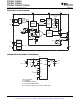
TPS62350, TPS62351 TPS62352, TPS62353 TPS62354, TPS62355, TPS62356 SLVS540E – MAY 2006 – REVISED APRIL 2008 .............................................................................................................................................................. www.ti.com DETAILED DESCRIPTION Operation The TPS6235x is a synchronous step-down converter typically operating with a 3-MHz fixed frequency pulse width modulation (PWM) at moderate to heavy load currents.
TPS62350, TPS62351 TPS62352, TPS62353 TPS62354, TPS62355, TPS62356 www.ti.com .............................................................................................................................................................. SLVS540E – MAY 2006 – REVISED APRIL 2008 Power-Save Mode : Light PFM With decreasing load current, the device can also automatically switch into light PFM pulse skipping operation in which the power stage operates intermittently based on load demand.
TPS62350, TPS62351 TPS62352, TPS62353 TPS62354, TPS62355, TPS62356 SLVS540E – MAY 2006 – REVISED APRIL 2008 .............................................................................................................................................................. www.ti.com This mechanism is used to limit the output current under short-circuit conditions. Therefore, the start-up time depends on the output capacitor and load current.
TPS62350, TPS62351 TPS62352, TPS62353 TPS62354, TPS62355, TPS62356 www.ti.com .............................................................................................................................................................. SLVS540E – MAY 2006 – REVISED APRIL 2008 THEORY OF OPERATION Serial Interface Description I2C is a 2-wire serial interface developed by Philips Semiconductor (see I2C-Bus Specification, Version 2.1, January 2000).
TPS62350, TPS62351 TPS62352, TPS62353 TPS62354, TPS62355, TPS62356 SLVS540E – MAY 2006 – REVISED APRIL 2008 .............................................................................................................................................................. www.ti.com The master then generates a repeated start condition (a repeated start condition has the same timing as the start condition).
TPS62350, TPS62351 TPS62352, TPS62353 TPS62354, TPS62355, TPS62356 www.ti.com ..............................................................................................................................................................
TPS62350, TPS62351 TPS62352, TPS62353 TPS62354, TPS62355, TPS62356 SLVS540E – MAY 2006 – REVISED APRIL 2008 .............................................................................................................................................................. www.ti.
TPS62350, TPS62351 TPS62352, TPS62353 TPS62354, TPS62355, TPS62356 www.ti.com .............................................................................................................................................................. SLVS540E – MAY 2006 – REVISED APRIL 2008 Voltage Scaling Management In order to reduce the power consumption of the processor core, the TPS6235x can scale its output voltage. There are two different strategies: 1) by software or 2) by hardware.
TPS62350, TPS62351 TPS62352, TPS62353 TPS62354, TPS62355, TPS62356 SLVS540E – MAY 2006 – REVISED APRIL 2008 .............................................................................................................................................................. www.ti.com In multiple-step mode, PWROK is defined as low while the output voltage is ramping up or down. Under all other operating conditions, PWROK is defined to be low when the output voltage is below -1.5% of the target value.
TPS62350, TPS62351 TPS62352, TPS62353 TPS62354, TPS62355, TPS62356 www.ti.com .............................................................................................................................................................. SLVS540E – MAY 2006 – REVISED APRIL 2008 REGISTER DESCRIPTION VSEL0 REGISTER (READ/WRITE) MSB 7 LSB 6 5 4 3 2 1 0 Memory location: 00 Reset state: X1XX XXXX – See the Ordering Information Table VOLTAGE STEP MULTIPLIER, VSM0 6-bit unsigned binary linear coding.
TPS62350, TPS62351 TPS62352, TPS62353 TPS62354, TPS62355, TPS62356 SLVS540E – MAY 2006 – REVISED APRIL 2008 .............................................................................................................................................................. www.ti.com CONTROL1 REGISTER (READ/WRITE) MSB 7 LSB 6 5 4 3 2 1 0 Memory location: 02 Reset state: 0001 0000 MODE0 This bit defines the mode of operation for VSEL low 0 : Light PFM with auto.
TPS62350, TPS62351 TPS62352, TPS62353 TPS62354, TPS62355, TPS62356 www.ti.com .............................................................................................................................................................. SLVS540E – MAY 2006 – REVISED APRIL 2008 CONTROL2 REGISTER (READ/WRITE) MSB 7 LSB 6 5 4 3 2 1 0 Memory location: 03 Reset state: 0000 0111 DEFSLEW DEFSLEW defines the output voltage ramp rate 000 : 0.15 mV/ms 001 : 0.3 mV/ms 010 : 0.6 mV/ms 011 : 1.
TPS62350, TPS62351 TPS62352, TPS62353 TPS62354, TPS62355, TPS62356 SLVS540E – MAY 2006 – REVISED APRIL 2008 .............................................................................................................................................................. www.ti.com APPLICATION INFORMATION Output Filter Design (Inductor and Output Capacitor) The TPS6235x step-down converter has an internal loop compensation.
TPS62350, TPS62351 TPS62352, TPS62353 TPS62354, TPS62355, TPS62356 www.ti.com .............................................................................................................................................................. SLVS540E – MAY 2006 – REVISED APRIL 2008 Table 5. List of Inductors MANUFACTURER SERIES DIMENSIONS FDK MIPSA2520 2.5 × 2.0 × 1.2 = 6 mm3 TDK VLF3010AT 2.8 × 2.6 × 1 = 7.28 mm3 LPS3010 3 × 3 × 1 = 9 mm3 LPS3015 3 × 3 × 1.5 = 13.
TPS62350, TPS62351 TPS62352, TPS62353 TPS62354, TPS62355, TPS62356 SLVS540E – MAY 2006 – REVISED APRIL 2008 .............................................................................................................................................................. www.ti.com Layout Considerations As for all switching power supplies, the layout is an important step in the design. High-speed operation of the TPS6235x device demands careful attention to PCB layout.
TPS62350, TPS62351 TPS62352, TPS62353 TPS62354, TPS62355, TPS62356 www.ti.com ..............................................................................................................................................................
PACKAGE OPTION ADDENDUM www.ti.
PACKAGE OPTION ADDENDUM www.ti.com 15-Apr-2008 (3) MSL, Peak Temp. -- The Moisture Sensitivity Level rating according to the JEDEC industry standard classifications, and peak solder temperature. Important Information and Disclaimer:The information provided on this page represents TI's knowledge and belief as of the date that it is provided. TI bases its knowledge and belief on information provided by third parties, and makes no representation or warranty as to the accuracy of such information.
PACKAGE MATERIALS INFORMATION www.ti.com 15-Apr-2008 TAPE AND REEL INFORMATION *All dimensions are nominal Device Package Package Pins Type Drawing SPQ Reel Reel Diameter Width (mm) W1 (mm) A0 (mm) B0 (mm) K0 (mm) P1 (mm) W Pin1 (mm) Quadrant TPS62351DRCR SON DRC 10 3000 330.0 12.4 3.3 3.3 1.6 8.0 12.0 Q2 TPS62351YZGR DSBGA YZG 12 3000 178.0 8.4 1.68 2.46 0.84 4.0 8.0 Q1 TPS62351YZGT DSBGA YZG 12 250 178.0 8.4 1.68 2.46 0.84 4.0 8.
PACKAGE MATERIALS INFORMATION www.ti.com 15-Apr-2008 *All dimensions are nominal Device Package Type Package Drawing Pins SPQ Length (mm) Width (mm) Height (mm) TPS62351DRCR SON DRC 10 3000 340.5 338.1 20.6 TPS62351YZGR DSBGA YZG 12 3000 195.2 193.7 34.9 TPS62351YZGT DSBGA YZG 12 250 195.2 193.7 34.9 TPS62353YZGR DSBGA YZG 12 3000 195.2 193.7 34.9 TPS62353YZGT DSBGA YZG 12 250 195.2 193.7 34.9 TPS62354YZGR DSBGA YZG 12 3000 195.2 193.7 34.
X: Max = 2292 µm, Min = 2192 µm Y: Max = 1524 µm, Min = 1424 µm
PACKAGE MATERIALS INFORMATION www.ti.com 24-Jan-2014 TAPE AND REEL INFORMATION *All dimensions are nominal Device Package Package Pins Type Drawing SPQ Reel Reel A0 Diameter Width (mm) (mm) W1 (mm) B0 (mm) K0 (mm) P1 (mm) TPS62350YZGR DSBGA YZG 12 3000 180.0 8.4 TPS62350YZGR DSBGA YZG 12 3000 180.0 TPS62350YZGT DSBGA YZG 12 250 180.
PACKAGE MATERIALS INFORMATION www.ti.com 24-Jan-2014 *All dimensions are nominal Device Package Type Package Drawing Pins SPQ Length (mm) Width (mm) Height (mm) TPS62350YZGR DSBGA YZG 12 3000 182.0 182.0 17.0 TPS62350YZGR DSBGA YZG 12 3000 220.0 220.0 34.0 TPS62350YZGT DSBGA YZG 12 250 220.0 220.0 34.0 TPS62350YZGT DSBGA YZG 12 250 182.0 182.0 17.0 TPS62351DRCR SON DRC 10 3000 340.5 338.1 20.6 TPS62351YZGR DSBGA YZG 12 3000 220.0 220.0 34.
IMPORTANT NOTICE Texas Instruments Incorporated and its subsidiaries (TI) reserve the right to make corrections, enhancements, improvements and other changes to its semiconductor products and services per JESD46, latest issue, and to discontinue any product or service per JESD48, latest issue. Buyers should obtain the latest relevant information before placing orders and should verify that such information is current and complete.