
Datasheet
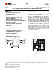
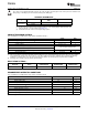
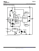
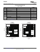

Table Of Contents
- FEATURES
- APPLICATIONS
- DESCRIPTION
- ABSOLUTE MAXIMUM RATINGS
- DISSIPATION RATINGS
- RECOMMENDED OPERATING CONDITIONS
- ELECTRICAL CHARACTERISTICS
- PIN ASSIGNMENT
- TYPICAL CHARACTERISTICS
- DETAILED DESCRIPTION
- Power Save Mode operation (MODE)
- Power Save Mode Transition Thresholds
- Output Voltage Tracking (OVT)
- Soft Start
- 100% Duty Cycle Low Dropout Operation
- Power Good
- Undervoltage Lockout
- Short-Circuit Protection
- Thermal Shutdown
- Input Capacitor Selection
- Output Filter Design (Inductor and Output Capacitor)
- Setting the Output Voltage Using the Feedback Resistor Divider
- Inductor Selection
- Layout Guidelines
- APPLICATION INFORMATION
1
FEATURES
DESCRIPTION
APPLICATIONS
V
I
1.8Vto3.8V
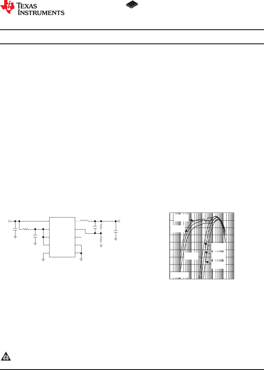
TPS62510
PGND
L1
2.2 Hm
C2
22 Fm
C3
22pF
R1
300kW
R2
200kW
Cf
100nF
Rf1 W
V
O
1.5Vto1.5 A
C1
22 Fm
SW
FB
PG
AGND
PVIN
7
AVIN
EN
OVT
MODE
10
5
6 8
9
2
1
4
3
95
50
90
80
70
60
85
75
65
55
0.01 0.1 1 10 10k
100
I -LoadCurrent-mA
L
Efficiency-%
1k
V =1.2V
O
V =1.9V
(ModeLow)
I
V =3.2V
(ModeHigh)
I
V =2.4V
(ModeHigh)
I
V =1.9V
(ModeHigh)
I
V =2.4V
(ModeLow)
I
V =3.2V
(ModeLow)
I
TPS62510
www.ti.com
................................................................................................................................................................ SLVS651A – MAY 2006 – REVISED JULY 2009
1.5-A, LOW V
I
HIGH EFFICIENCY STEP-DOWN CONVERTER
2
• 1.8-V to 3.8-V Input Voltage Range
• Up to 96% High Efficiency Synchronous
The TPS62510 family are high-efficiency step-down
converters targeted for operation from a 1.8-V to
Step-Down Converter
3.8-V input voltage rail, ideally suited for 2-cell
• 1.5-MHz Fixed Frequency PWM Operation
Alkaline or NiMHd applications. The TPS62510 is
• 1% Output Voltage Accuracy in Fixed
also ideal as a point-of-load regulator running from a
Frequency PWM Mode
fixed 3.3-V, 2.5-V or 1.8-V input voltage rail. The
converter operates in fixed frequency PWM mode
• Power Save Mode Operation for High
switching at 1.5 MHz with the MODE pin high. Pulling
Efficiency Over the Entire Load Current Range
the MODE pin low enables the high efficiency mode.
• 22- µ A Quiescent Current
In high efficiency mode, the device operates with a
• Fixed and Adjustable Output Voltage
1.5 MHz fixed frequency PWM at nominal load
current, and automatically enters the Power Save
• Output Voltage Tracking (OVT) for Reliable
Mode at light load currents. For maximum system
Sequencing
reliability, the converter features Output Voltage
• Available in a 10-Pin QFN (3 x 3 mm) Package
Tracking using the OVT pin to allow sequencing, and
to allow for the output voltage to track an external
voltage applied to this pin.
• Portable Devices (Mobile Phone, PDA)
• 2-Cell NiMHd/Alkaline Applications
• Hard Disc Drives
• Point-Of-Load Regulation
• Notebook Computers
• WiMAX and WLAN Applications
Figure 1. Typical Application Figure 2. Efficiency vs Load Current
1
Please be aware that an important notice concerning availability, standard warranty, and use in critical applications of Texas
Instruments semiconductor products and disclaimers thereto appears at the end of this data sheet.
2 PowerPAD is a trademark of Texas Instruments.
PRODUCTION DATA information is current as of publication date.
Copyright © 2006 – 2009, Texas Instruments Incorporated
Products conform to specifications per the terms of the Texas
Instruments standard warranty. Production processing does not
necessarily include testing of all parameters.