
Datasheet
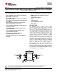
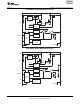
Table Of Contents
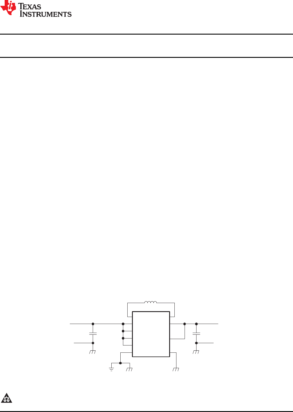
L1
VIN
VINA
EN
PS/SYNC
GND
L2
VOUT
FB
PGND
L1
1.5µH
C2
10µ
F
C1
4.7µF
V
IN
1.8Vto
5.5V
V
OUT
3.3Vupto
800mA
TPS63031
TPS63030
TPS63031
www.ti.com
SLVS696B –OCTOBER 2008–REVISED MARCH 2012
HIGH EFFICIENCY SINGLE INDUCTOR BUCK-BOOST CONVERTER WITH 1-A SWITCHES
Check for Samples: TPS63030, TPS63031
1
FEATURES
APPLICATIONS
2
• Up to 96% Efficiency
• All Two-Cell and Three-Cell Alkaline, NiCd or
NiMH or Single-Cell Li Battery Powered
• 800-mA Output Current at 3.3V in Step Down
Products
Mode (VIN = 3.6V to 5.5V)
• Portable Audio Players
• Up to 500-mA Output Current at 3.3V in Boost
Mode (VIN > 2.4V) • PDAs
• Automatic Transition Between Step Down and • Cellular Phones
Boost Mode
• Personal Medical Products
• Device Quiescent Current less than 50μA
• White LEDs
• Input Voltage Range: 1.8V to 5.5V
DESCRIPTION
• Fixed and Adjustable Output Voltage Options
The TPS6303x devices provide a power supply
from 1.2V to 5.5V
solution for products powered by either a two-cell or
• Power Save Mode for Improved Efficiency at
three-cell alkaline, NiCd or NiMH battery, or a one-
Low Output Power
cell Li-Ion or Li-polymer battery. Output currents can
• Forced Fixed Frequency Operation and
go as high as 600 mA while using a single-cell Li-Ion
Synchronization Possible
or Li-Polymer Battery, and discharge it down to 2.5V
or lower. The buck-boost converter is based on a
• Load Disconnect During Shutdown
fixed frequency, pulse-width-modulation (PWM)
• Over-Temperature Protection
controller using synchronous rectification to obtain
• Available in Small 2.5mm × 2.5mm, QFN-10
maximum efficiency. At low load currents, the
Package
converter enters Power Save mode to maintain high
efficiency over a wide load current range. The Power
Save mode can be disabled, forcing the converter to
operate at a fixed switching frequency. The maximum
average current in the switches is limited to a typical
value of 1000 mA. The output voltage is
programmable using an external resistor divider, or is
fixed internally on the chip. The converter can be
disabled to minimize battery drain. During shutdown,
the load is disconnected from the battery. The device
is packaged in a 10-pin QFN PowerPAD™ package
measuring 2.5mm × 2.5 mm (DSK).
1
Please be aware that an important notice concerning availability, standard warranty, and use in critical applications of
Texas Instruments semiconductor products and disclaimers thereto appears at the end of this data sheet.
2PowerPAD is a trademark of Texas Instruments.
PRODUCTION DATA information is current as of publication date.
Copyright © 2008–2012, Texas Instruments Incorporated
Products conform to specifications per the terms of the Texas
Instruments standard warranty. Production processing does not
necessarily include testing of all parameters.