
Datasheet
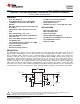
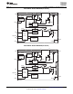
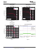

V
IN
L1
VIN
VAUX
EN
PS/SYNC
GND
L2
VOUT
FB
PGND
L
1
1µH
C
2
C
3
2.5 V to
12V
V
OUT
5V
/800mA
TPS63060
PG
Power Good
Output
C
1
2X10µF
0.1µF
3X22µF
1MΩ
111kΩ
10pF
R
1
R
2
C
4
1MΩ
R
3
TPS63060
TPS63061
www.ti.com
SLVSA92A –DECEMBER 2011–REVISED FEBRUARY 2012
HIGH INPUT VOLTAGE BUCK-BOOST CONVERTER WITH 2A SWITCH CURRENT
Check for Samples: TPS63060, TPS63061
1
FEATURES
2
• Up to 93% Efficiency
• Load Disconnect During Shutdown
• 2A/1A Output Current at 5V in Buck Mode • Overtemperature Protection
• 1.3A Output Current at 5V in Boost Mode • Overvoltage Protection
(VIN>4V)
• Available in a 3-mm × 3-mm, SON-10 Package
• Automatic Transition Between Step Down and
Boost Mode APPLICATIONS
• Typical Device Quiescent Current less than
• Dual LI-Ion Application
30μA
• DSC's and Camcorders
• Input Voltage Range: 2.5V to 12V
• Notebook Computer
• Fixed and Adjustable Output Voltage Options
• Industrial Metering Equipment
from 2.5V to 8V
• Ultra Mobile PC's and Mobile Internet Devices
• Power Save Mode for Improved Efficiency at
• Personal Medical Products
Low Output Power
• High Power LED's
• Forced Fixed Frequency Operation at 2.4MHz
and Synchronization Possible
• Power Good Output
• Buck-Boost Overlap Control™
DESCRIPTION
The TPS6306x devices provide a power supply solution for products powered by either three-cell up to six-cell
alkaline, NiCd or NiMH battery, or a one-cell or dual-cell Li-Ion or Li-polymer battery. Output currents can go as
high as 2A while using a dual-cell Li-Ion or Li-Polymer Battery, and discharge it down to 5V or lower. The
buck-boost converter is based on a fixed frequency, pulse-width-modulation (PWM) controller using synchronous
rectification to obtain maximum efficiency. At low load currents, the converter enters Power Save mode to
maintain high efficiency over a wide load current range. The Power Save mode can be disabled, forcing the
converter to operate at a fixed switching frequency. The maximum average current in the switches is limited to a
typical value of 2.25A. The output voltage is programmable using an external resistor divider, or is fixed internally
on the chip. The converter can be disabled to minimize battery drain. During shutdown, the load is disconnected
from the battery. The device is packaged in a 10-pin SON PowerPAD™ package measuring 3mm × 3mm (DSC).
1
Please be aware that an important notice concerning availability, standard warranty, and use in critical applications of Texas
Instruments semiconductor products and disclaimers thereto appears at the end of this data sheet.
2Buck-Boost Overlap Control, PowerPAD are trademarks of Texas Instruments.
PRODUCTION DATA information is current as of publication date.
Copyright © 2011–2012, Texas Instruments Incorporated
Products conform to specifications per the terms of the Texas
Instruments standard warranty. Production processing does not
necessarily include testing of all parameters.