
Datasheet


User's Guide
SLVU357–March 2010
Using the TPS650001/3/6 2.25 MHz Step-Down Converter
with Dual LDO
The TPS650001/3/6 is a single chip Power Management ICs for portable applications. The device
combines a single step-down converter with two low dropout regulators. The step-down converter enters a
low power mode at light load for maximum efficiency across the widest possible range of load currents.
For low noise applications the device can be forced into fixed frequency PWM mode. The step-down
converter allows the use of a small inductor and capacitors to achieve a small solution size. The
step-down converter has Power Good status output that can be used for sequencing. The LDOs are
capable of supplying 300mA and can operate with an input voltage range between 1.6V and 6.0V,
allowing them to be supplied from the step-down converter or directly from the main battery. The
step-down converter and the LDOs have separate voltage inputs and enables, allowing for design and
sequencing flexibility.
Contents
1 Introduction .................................................................................................................. 2
1.1 Applications ......................................................................................................... 2
1.2 Features ............................................................................................................. 2
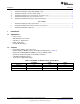
2 TPS650001/3/6 EVM Electrical Performance Specifications .......................................................... 3
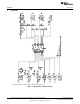
3 Schematic .................................................................................................................... 4
4 Connector and Test Point Description ................................................................................... 5
4.1 JP1 – ENDCDC .................................................................................................... 5
4.2 JP2 – ENLDO1 ..................................................................................................... 5
4.3 JP3 – ENLDO2 ..................................................................................................... 5
4.4 JP4 – MODE ........................................................................................................ 5
4.5 JP5 – VINLDO1 .................................................................................................... 5
4.6 JP6 – VINLOD2 .................................................................................................... 5
4.7 J1 – VIN/GND ...................................................................................................... 5
4.8 J2 – VODCDC/GND ............................................................................................... 5
4.9 J3 – VLDO1/GND .................................................................................................. 6
4.10 J4 – VLDO2/GND .................................................................................................. 6
4.11 J5 – PG .............................................................................................................. 6
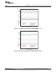
5 4 TPS650001/3/6 Typical Performance Data and Characteristic Curves ........................................... 6
5.1 Efficiency ............................................................................................................ 6
5.2 Line and Load Regulation ......................................................................................... 6
5.3 Output Voltage Ripple ............................................................................................. 9
5.4 Startup Timing .................................................................................................... 10
6 EVM Assembly Drawings and Layout .................................................................................. 11
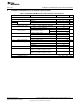
7 List of Materials ............................................................................................................ 14
List of Figures
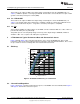
1 TPS650001/3/6 EVM Schematic.......................................................................................... 4
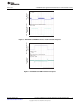
2 TPS650001/3/6 Efficiency vs Load Current ............................................................................. 6
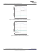
3 TPS650001/3/6 DCDC Converter Load Transient Response......................................................... 7
4 TPS650001/3/6 LDOx Transient Response ............................................................................. 7
5 TPS650001/3/6 DCDC Converter Line Transient Response.......................................................... 8
6 TPS650001/3/6 LDOx Line Transient Response ....................................................................... 8
1
SLVU357–March 2010 Using the TPS650001/3/6 2.25 MHz Step-Down Converter with Dual LDO
Submit Documentation Feedback
Copyright © 2010, Texas Instruments Incorporated