TPS65023, TPS65023B SLVS670J – JUNE 2006 – REVISED SEPTEMBER 2011 www.ti.com POWER MANAGEMENT IC FOR LI-ION POWERED SYSTEMS Check for Samples: TPS65023, TPS65023B FEATURES 1 • 23 • • • • • • • • • • • • • • • 1.7 A, 90% Efficient Step-Down Converter for Processor Core (VDCDC1) 1.2 A, Up to 95% Efficient Step-Down Converter for System Voltage (VDCDC2) 1.
TPS65023, TPS65023B SLVS670J – JUNE 2006 – REVISED SEPTEMBER 2011 www.ti.com These devices have limited built-in ESD protection. The leads should be shorted together or the device placed in conductive foam during storage or handling to prevent electrostatic damage to the MOS gates.
TPS65023, TPS65023B SLVS670J – JUNE 2006 – REVISED SEPTEMBER 2011 www.ti.com RECOMMENDED OPERATING CONDITIONS over operating free-air temperature range (unless otherwise noted) MIN NOM MAX Input voltage range step-down converters (VINDCDC1, VINDCDC2, VINDCDC3); pins need to be tied to the same voltage rail 2.5 6 Output voltage range for VDCDC1 step-down converter (1) 0.6 VINDCDC1 (1) 0.6 VINDCDC2 Output voltage range for VDCDC3 step-down converter (1) 0.
TPS65023, TPS65023B SLVS670J – JUNE 2006 – REVISED SEPTEMBER 2011 www.ti.com ELECTRICAL CHARACTERISTICS VINDCDC1 = VINDCDC2 = VINDCDC3 = VCC = VINLDO = 3.6 V, VBACKUP = 3 V, TA = –40°C to 85°C, typical values are at TA = 25°C (unless otherwise noted) PARAMETER TEST CONDITIONS MIN TYP MAX UNIT CONTROL SIGNALS : SCLK, SDAT (input) for TPS65023 VIH High level input voltage (except the SDAT pin) Resistor pullup at SCLK = 4.7kΩ, pulled to VRTC 1.
TPS65023, TPS65023B SLVS670J – JUNE 2006 – REVISED SEPTEMBER 2011 www.ti.com ELECTRICAL CHARACTERISTICS VINDCDC1 = VINDCDC2 = VINDCDC3 = VCC = VINLDO = 3.6 V, VBACKUP = 3 V, TA = –40°C to 85°C, typical values are at TA = 25°C (unless otherwise noted) PARAMETER TEST CONDITIONS MIN TYP MAX UNIT SUPPLY PINS: VCC, VINDCDC1, VINDCDC2, VINDCDC3 I(q) II I(q) Operating quiescent current, PFM Current into VCC; PWM Quiescent current All 3 DCDC converters enabled, zero VCC = 3.
TPS65023, TPS65023B SLVS670J – JUNE 2006 – REVISED SEPTEMBER 2011 www.ti.com ELECTRICAL CHARACTERISTICS VINDCDC1 = VINDCDC2 = VINDCDC3 = VCC = VINLDO = 3.6 V, VBACKUP = 3 V, TA = –40°C to 85°C, typical values are at TA = 25°C (unless otherwise noted) PARAMETER TEST CONDITIONS MIN TYP MAX UNIT 20 33 μA 3 μA SUPPLY PINS: VBACKUP, VSYSIN, VRTC I(q) Operating quiescent current VBACKUP = 3 V, VSYSIN = 0 V; VCC = 2.
TPS65023, TPS65023B SLVS670J – JUNE 2006 – REVISED SEPTEMBER 2011 www.ti.com ELECTRICAL CHARACTERISTICS VINDCDC1 = VINDCDC2 = VINDCDC3 = VCC = VINLDO = 3.6 V, VBACKUP = 3 V, TA = –40°C to 85°C, typical values are at TA = 25°C (unless otherwise noted) PARAMETER TEST CONDITIONS MIN TYP MAX UNIT VDCDC1 STEP-DOWN CONVERTER VI Input voltage range, VINDCDC1 IO Maximum output current I(SD) Shutdown supply current in VINDCDC1 DCDC1_EN = GND 0.
TPS65023, TPS65023B SLVS670J – JUNE 2006 – REVISED SEPTEMBER 2011 www.ti.com ELECTRICAL CHARACTERISTICS VINDCDC1 = VINDCDC2 = VINDCDC3 = VCC = VINLDO = 3.6 V, VBACKUP = 3 V, TA = –40°C to 85°C, typical values are at TA = 25°C (unless otherwise noted) PARAMETER TEST CONDITIONS MIN TYP MAX UNIT VDCDC2 STEP-DOWN CONVERTER VI Input voltage range, VINDCDC2 2.5 DEFDCDC2 = GND 1200 1000 6 V IO Maximum output current VINDCDC2 = 3.6 V; 3.3 V - 1% ≤ VDCDC2 ≤ 3.
TPS65023, TPS65023B SLVS670J – JUNE 2006 – REVISED SEPTEMBER 2011 www.ti.com ELECTRICAL CHARACTERISTICS VINDCDC1 = VINDCDC2 = VINDCDC3 = VCC = VINLDO = 3.6 V, VBACKUP = 3 V, TA = –40°C to 85°C, typical values are at TA = 25°C (unless otherwise noted) PARAMETER TEST CONDITIONS MIN TYP MAX UNIT VDCDC3 STEP-DOWN CONVERTER VI Input voltage range, VINDCDC3 2.5 DEFDCDC3 = GND 6 V 1000 IO Maximum output current VINDCDC3 = 3.6 V; 3.3V - 1% ≤ VDCDC3 ≤ 3.
TPS65023, TPS65023B SLVS670J – JUNE 2006 – REVISED SEPTEMBER 2011 www.ti.com ELECTRICAL CHARACTERISTICS VINDCDC1 = VINDCDC2 = VINDCDC3 = VCC = VINLDO = 3.6 V, VBACKUP = 3 V, TA = –40°C to 85°C, typical values are at TA = 25°C (unless otherwise noted) PARAMETER TEST CONDITIONS MIN TYP MAX UNIT VLDO1 and VLDO2 LOW DROPOUT REGULATORS VI Input voltage range for LDO1, 2 1.5 6.5 V VO(LD01) LDO1 output voltage range 1 3.15 V VO(LDO2) LDO2 output voltage range 1 3.
TPS65023, TPS65023B SLVS670J – JUNE 2006 – REVISED SEPTEMBER 2011 www.ti.
TPS65023, TPS65023B SLVS670J – JUNE 2006 – REVISED SEPTEMBER 2011 www.ti.com PIN FUNCTIONS (continued) PIN NAME NO. I/O DESCRIPTION VCC 37 I Power supply for digital and analog circuitry of VDCDC1, VDCDC2, and VDCDC3 dc-dc converters. VCC must be connected to the same voltage supply as VINDCDC3, VINDCDC1, and VINDCDC2. VCC also supplies serial interface block. DEFDCDC1 10 I Input signal indicating default VDCDC1 voltage, 0 = 1.2 V, 1 = 1.
TPS65023, TPS65023B SLVS670J – JUNE 2006 – REVISED SEPTEMBER 2011 www.ti.
TPS65023, TPS65023B SLVS670J – JUNE 2006 – REVISED SEPTEMBER 2011 www.ti.com TYPICAL CHARACTERISTICS Graphs were taken using the EVM with the following inductor/output capacitor combinations: CONVERTER INDUCTOR OUTPUT CAPACITOR OUTPUT CAPACITOR VALUE VDCDC1 VLCF4020-2R2 C2012X5R0J106M 2 × 10 μF VDCDC2 VLCF4020-2R2 C2012X5R0J106M 2 × 10 μF VDCDC3 VLF4012AT-2R2M1R5 C2012X5R0J106M 2 × 10 μF Table 1.
TPS65023, TPS65023B SLVS670J – JUNE 2006 – REVISED SEPTEMBER 2011 www.ti.com DCDC2: EFFICIENCY vs OUTPUT CURRENT 100 90 DCDC2: EFFICIENCY vs OUTPUT CURRENT 100 VI = 2.5 V VI = 3.6 V 80 80 60 VI = 5 V 40 30 TA = 25°C VO = 1.8 V PWM/PFM Mode 10 0.1 100 50 40 1 10 100 IO - Output Current - mA 1k 0 0.01 10 k 0.1 Figure 4. DCDC3: EFFICIENCY vs OUTPUT CURRENT DCDC3: EFFICIENCY vs OUTPUT CURRENT 100 80 80 TA = 25°C VO = 1.
TPS65023, TPS65023B SLVS670J – JUNE 2006 – REVISED SEPTEMBER 2011 www.ti.com DCDC2: OUTPUT VOLTAGE vs OUTPUT CURRENT at 85°C 3.354 DCDC3: OUTPUT VOLTAGE vs OUTPUT CURRENT at 85°C TA = 85°C DEFDCDC2 = VINDCDC2 3.334 3.314 VO - Output Voltage - V VO - Output Voltage - V 3.334 VI = 3.8 V 3.294 VI = 3.7 V 3.274 3.254 3.234 0.1 TA = 85°C DEFDCDC3 = VINDCDC3 3.354 VI = 3.5 V VI = 3.6 V 3.314 VI = 4 V 3.294 VI = 3.5 V 3.274 VI = 3.9 V VI = 3.8 V VI = 3.6 V VI = 3.7 V 3.
TPS65023, TPS65023B SLVS670J – JUNE 2006 – REVISED SEPTEMBER 2011 www.ti.com VDCDC3 LINE TRANSIENT RESPONSE VDCDC1 LOAD TRANSIENT RESPONSE VINDCDC3 C1 High 4.20 V C1 Low 3.59 V C2 Pk-Pk 60.4 mV VDCDC3 C2 Mean 3.28264 V IO = 100 mA VINDCDC3 = 3.6 V - 4.2 V DEFDCDC3 = VINDCDC3 PWW Mode Figure 11. Figure 12. VDCDC2 LOAD TRANSIENT RESPONSE VDCDC3 LOAD TRANSIENT RESPONSE VDCDC3 = 3.3 V @ 50 mV/Div (AC Coupled) ILOAD @ 500 mA/Div 800 mA 100 mA VIN = 3.8 V Figure 13.
TPS65023, TPS65023B SLVS670J – JUNE 2006 – REVISED SEPTEMBER 2011 www.ti.com VDCDC2 OUTPUT VOLTAGE RIPPLE VDCDC2 OUTPUT VOLTAGE RIPPLE Figure 15. Figure 16. VDCDC2 OUTPUT VOLTAGE RIPPLE STARTUP VDCDC1, VDCDC2, AND VDCDC3 mV Figure 17. 18 Submit Documentation Feedback Figure 18.
TPS65023, TPS65023B SLVS670J – JUNE 2006 – REVISED SEPTEMBER 2011 www.ti.com STARTUP LDO1 AND LDO2 LDO1 LINE TRANSIENT RESPONSE ENABLE IO = 25 mA VO = 1.1 V o TA = 25 C Ch1 = VI Ch2 = VO C1 High 3.83 V C1 Low 3.29 V LDO1 C2 PK-PK 6.2 mV C2 Mean 1.09702 V LDO2 Ch1 = VI Ch2 = VO Figure 19. Figure 20. LDO2 LINE TRANSIENT RESPONSE VRTC LINE TRANSIENT RESPONSE IO = 25 mA VO = 3.3 V TA = 25oC C1 High 4.51 V Ch1 = VI Ch2 = VO IO = 10 mA VO = 3 V o TA = 25 C C1 High 3.82 V C1 Low 3.
TPS65023, TPS65023B SLVS670J – JUNE 2006 – REVISED SEPTEMBER 2011 www.ti.com LDO1 LOAD TRANSIENT RESPONSE LDO2 LOAD TRANSIENT RESPONSE C4 High 47.8 mA C4 High 48.9 mA C4 Low -2.9 mA C4 Low 2.1 mA C2 PK-PK 40.4 mV C2 PK-PK 42.5 mV C2 Mean 3.29821 V C2 Mean 1.09664 V Ch2 = VO Ch4 = IO VI = 3.3 V VO = 1.1 V o TA = 25 C VI = 4 V VO = 3.3 V o TA = 25 C Ch2 = VO Ch4 = IO Figure 23. Figure 24. VRTC LOAD TRANSIENT RESPONSE C4 High 21.4 mA C4 Low -1.4 mA C2 PK-PK 76 mV C2 Mean 2.
TPS65023, TPS65023B SLVS670J – JUNE 2006 – REVISED SEPTEMBER 2011 www.ti.com DETAILED DESCRIPTION VRTC OUTPUT AND OPERATION WITH OR WITHOUT BACKUP BATTERY The VRTC pin is an always-on output, intended to supply up to 30 mA to a permanently required rail (i.e. for a Real Time Clock). The TPS65023, TPS65023B asserts the RESPWRON signal if VRTC drops below 2.4 V. VRTC is selected from a priority scheme based on the VSYSIN and VBACKUP inputs. When the voltage at the VSYSIN pin exceeds 2.
TPS65023, TPS65023B SLVS670J – JUNE 2006 – REVISED SEPTEMBER 2011 VSYSIN Vref V_VSYSIN priority #1 www.ti.com VCC VBACKUP Vref V_VBACKUP priority #2 V_VSYSIN V_VBACKUP EN VRTC LDO priority #3 VRTC RESPWRON Vref A. V_VSYSIN, V_VBACKUP thresholds: falling = 2.55 V, rising = 2.65 V ±3% B. RESPWRON thresholds: falling = 2.4 V, rising = 2.52 V ±3% Figure 26.
TPS65023, TPS65023B SLVS670J – JUNE 2006 – REVISED SEPTEMBER 2011 www.ti.com During PWM operation, the converters use a unique fast response voltage mode controller scheme with input voltage feed-forward to achieve good line and load regulation allowing the use of small ceramic input and output capacitors. At the beginning of each clock cycle initiated by the clock signal, the P-channel MOSFET switch is turned on.
TPS65023, TPS65023B SLVS670J – JUNE 2006 – REVISED SEPTEMBER 2011 www.ti.com These control methods reduce the quiescent current to typically 14 μA per converter, and the switching activity to a minimum, thus achieving the highest converter efficiency. Setting the comparator thresholds at the nominal output voltage at light load current results in a low output voltage ripple. The ripple depends on the comparator delay and the size of the output capacitor.
TPS65023, TPS65023B SLVS670J – JUNE 2006 – REVISED SEPTEMBER 2011 www.ti.com LOW DROPOUT VOLTAGE REGULATORS The low dropout voltage regulators are designed to operate well with low value ceramic input and output capacitors. They operate with input voltages down to 1.5 V. The LDOs offer a maximum dropout voltage of 300 mV at rated output current. Each LDO supports a current limit feature.
TPS65023, TPS65023B SLVS670J – JUNE 2006 – REVISED SEPTEMBER 2011 www.ti.com SYSTEM RESET + CONTROL SIGNALS The RESPWRON signal can be used as a global reset for the application. It is an open drain output. The RESPWRON signal is generated according to the power good comparator of VRTC, and remains low for tnrespwron seconds after VRTC has risen above 2.52 V (falling threshold is 2.4 V, 5% hysteresis). tnrespwron is set by an external capacitor at the TRESPWRON pin. 1 nF gives typically 100 ms.
TPS65023, TPS65023B SLVS670J – JUNE 2006 – REVISED SEPTEMBER 2011 www.ti.com TIMING DIAGRAMS Figure 27. HOT_RESET Timing VCC 2.35V 1.9V 1.2V 2.47V 1.9V 0.8V UVLO* VRTC 2.52V 2.4V 3.0V RESPWRON tNRESPWRON DCDCx_EN Ramp within 800 μs VO DCDCx slope depending on load LDO_EN VO LDOx VSYSIN=VBACKUP=GND; VINLDO=VCC *... internal signal Figure 28.
TPS65023, TPS65023B SLVS670J – JUNE 2006 – REVISED SEPTEMBER 2011 www.ti.com Figure 29. DVS Timing SERIAL INTERFACE The serial interface is compatible with the standard and fast mode I2C specifications, allowing transfers at up to 400 kHz. The interface adds flexibility to the power supply solution, enabling most functions to be programmed to new values depending on the instantaneous application requirements and charger status to be monitored.
TPS65023, TPS65023B SLVS670J – JUNE 2006 – REVISED SEPTEMBER 2011 www.ti.com For normal data transfer, DATA is allowed to change only when CLK is low. Changes when CLK is high are reserved for indicating the start and stop conditions. During data transfer, the data line must remain stable whenever the clock line is high. There is one clock pulse per bit of data. Each data transfer is initiated with a start condition and terminated with a stop condition.
TPS65023, TPS65023B SLVS670J – JUNE 2006 – REVISED SEPTEMBER 2011 www.ti.com SCLK SDAT A6 Start A0 R/W ACK 0 0 R0 R7 A6 ACK A0 R/W ACK 1 0 0 Register Address Slave Address D0 D7 ACK Slave Drives the Data Slave Address Stop Master Drives ACK and Stop Repeated Start Note: SLAVE = TPS65023 Figure 33.
TPS65023, TPS65023B SLVS670J – JUNE 2006 – REVISED SEPTEMBER 2011 www.ti.com Table 4.
TPS65023, TPS65023B SLVS670J – JUNE 2006 – REVISED SEPTEMBER 2011 www.ti.com PGOODZ.
TPS65023, TPS65023B SLVS670J – JUNE 2006 – REVISED SEPTEMBER 2011 www.ti.com MASK.
TPS65023, TPS65023B SLVS670J – JUNE 2006 – REVISED SEPTEMBER 2011 www.ti.com CON_CTRL.
TPS65023, TPS65023B SLVS670J – JUNE 2006 – REVISED SEPTEMBER 2011 www.ti.com CON_CTRL2. Register Address: 05h (read/write) CON_CTRL2 Bit name and function Default Default value loaded by: Read/Write B7 B6 GO Core adj allowed B5 0 1 UVLO + DONE RESET(1) 0 R/W R/W Default Value: 40h B4 0 B3 B2 B1 B0 DCDC2 discharge DCDC1 discharge DCDC3 discharge 0 0 0 UVLO UVLO UVLO R/W R/W R/W 0 The CON_CTRL2 register can be used to take control the inductive converters.
TPS65023, TPS65023B SLVS670J – JUNE 2006 – REVISED SEPTEMBER 2011 www.ti.com DEFCORE.
TPS65023, TPS65023B SLVS670J – JUNE 2006 – REVISED SEPTEMBER 2011 www.ti.com DEFSLEW. Register Address: 07h (read/write) DEFSLEW B7 B6 Default Value: 06h B5 B4 B3 Bit name and function B2 B1 B0 SLEW2 SLEW1 SLEW0 1 1 0 UVLO UVLO UVLO R/W R/W R/W Default Default value loaded by: Read/Write SLEW2 SLEW1 SLEW0 VDCDC1 SLEW RATE 0 0 0 0.225 mV/μs 0 0 1 0.45 mV/μs 0 1 0 0.9 mV/μs 0 1 1 1.8 mV/μs 1 0 0 3.6 mV/μs 1 0 1 7.2 mV/μs 1 1 0 14.
TPS65023, TPS65023B SLVS670J – JUNE 2006 – REVISED SEPTEMBER 2011 www.ti.com LDO_CTRL.
TPS65023, TPS65023B SLVS670J – JUNE 2006 – REVISED SEPTEMBER 2011 www.ti.com A conservative approach is to select the inductor current rating just for the maximum switch current of the TPS65023, TPS65023B (2 A for the VDCDC1 and VDCDC2 converters, and 1.5 A for the VDCDC3 converter). The core material from inductor to inductor differs and has an impact on the efficiency especially at high switching frequencies. See Table 5 and the typical applications for possible inductors. Table 5.
TPS65023, TPS65023B SLVS670J – JUNE 2006 – REVISED SEPTEMBER 2011 www.ti.com Table 6.
TPS65023, TPS65023B SLVS670J – JUNE 2006 – REVISED SEPTEMBER 2011 www.ti.com VRTC Output It is required that a 4.7-μF (minimum) capacitor be added to the VRTC pin even if the output is not used. LDO1 and LDO2 The LDOs in the TPS65023, TPS65023B are general-purpose LDOs which are stable using ceramics capacitors. The minimum output capacitor required is 2.2 μF. The LDOs output voltage can be changed to different voltages between 1 V and 3.3 V using the I2C interface.
TPS65023, TPS65023B SLVS670J – JUNE 2006 – REVISED SEPTEMBER 2011 www.ti.com APPLICATION INFORMATION Layout Considerations As for all switching power supplies, the layout is an important step in the design. Proper function of the device demands careful attention to PCB layout. Care must be taken in board layout to get the specified performance. If the layout is not carefully done, the regulators may show poor line and/or load regulation, and stability issues as well as EMI problems.
TPS65023, TPS65023B SLVS670J – JUNE 2006 – REVISED SEPTEMBER 2011 www.ti.com Typical Configuration for the Texas Instruments® TMS320DM644x DaVinci Processors Reset Condition of DCDC1 If DEFDCDC1 is connected to ground and DCDC1_EN is pulled high after VINDCDC1 is applied, the output voltage of DCDC1 defaults to 1.225V instead of 1.2V (high by 2%). Figure 37 illustrates the problem. VCC/VINDCDC1 DCDC1_EN 1.225 V 1.225 V 1.225 V VDCDC1 Figure 37.
TPS65023, TPS65023B SLVS670J – JUNE 2006 – REVISED SEPTEMBER 2011 www.ti.com VCC/VINDCDC1 DCDC1_EN 1.20 V 1.20 V 1.20 V VDCDC1 Figure 38. Workaround 1 Workaround 2: Write the correct voltage to the DEF_CORE register via I2C. This can be done before or after the converter is enabled. If written before the enable, the only bit changed is DEF_CORE[0]. The voltage will be 1.2V, however, when the enable is pulled high (Figure 39). VCC/VINDCDC1 DCDC1_EN I2C Bus DEF_CORE ?? 0x1F 0x11 1.
TPS65023, TPS65023B SLVS670J – JUNE 2006 – REVISED SEPTEMBER 2011 www.ti.com CHANGES OF TPS65023B VERSUS TPS65023 ITEM VIH DESCRIPTION Reference High level input voltage for the SDAT pin VIH High level input voltage for the SCLK pin VIL Low level input voltage for SCLK and SDAT pin th(DATA) Data input hold time tsu(DATA) Data input setup time ELECTRICAL CHARACTERISTICS Table 4 TPS65023 TPS65023B Minimum 1.3V Minimum 1.69V; Vcc = 2.5V to 5.25V Minimum 1.55V; Vcc = 2.5V to 4.5V Minimum 1.
TPS65023, TPS65023B SLVS670J – JUNE 2006 – REVISED SEPTEMBER 2011 www.ti.com REVISION HISTORY Changes from Original (May 2006) to Revision A Page • Changed VDCDC1 STEP-DOWN CONVERTER Electrical Characteristics ........................................................................ 7 • Changed VDCDC3 STEP-DOWN CONVERTER Electrical Characteristics ........................................................................
TPS65023, TPS65023B SLVS670J – JUNE 2006 – REVISED SEPTEMBER 2011 www.ti.com Changes from Revision E (January 2007) to Revision F • Page Changed text string from: "If it is tied to VCC, the default is 2.5 V" To: "If it is tied to VCC, the default is 3.3 V" ............. 22 Changes from Revision F (July 2007) to Revision G • Page Changed the Interrupt Management and the INT Pin section. ...........................................................................................
PACKAGE OPTION ADDENDUM www.ti.
PACKAGE OPTION ADDENDUM www.ti.com 19-Sep-2012 In no event shall TI's liability arising out of such information exceed the total purchase price of the TI part(s) at issue in this document sold by TI to Customer on an annual basis.
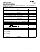
PACKAGE MATERIALS INFORMATION www.ti.com 14-Jul-2012 TAPE AND REEL INFORMATION *All dimensions are nominal Device Package Package Pins Type Drawing TPS65023BRSBR WQFN RSB 40 TPS65023BRSBT WQFN RSB TPS65023RSBR WQFN RSB TPS65023RSBT WQFN RSB SPQ Reel Reel A0 Diameter Width (mm) (mm) W1 (mm) B0 (mm) K0 (mm) P1 (mm) W Pin1 (mm) Quadrant 3000 330.0 12.4 5.3 5.3 1.5 8.0 12.0 Q2 40 250 180.0 12.4 5.3 5.3 1.5 8.0 12.0 Q2 40 3000 330.0 12.4 5.3 5.3 1.5 8.0 12.
PACKAGE MATERIALS INFORMATION www.ti.com 14-Jul-2012 *All dimensions are nominal Device Package Type Package Drawing Pins SPQ Length (mm) Width (mm) Height (mm) TPS65023BRSBR WQFN RSB 40 3000 367.0 367.0 35.0 TPS65023BRSBT WQFN RSB 40 250 210.0 185.0 35.0 TPS65023RSBR WQFN RSB 40 3000 367.0 367.0 35.0 TPS65023RSBT WQFN RSB 40 250 210.0 185.0 35.
IMPORTANT NOTICE Texas Instruments Incorporated and its subsidiaries (TI) reserve the right to make corrections, enhancements, improvements and other changes to its semiconductor products and services per JESD46, latest issue, and to discontinue any product or service per JESD48, latest issue. Buyers should obtain the latest relevant information before placing orders and should verify that such information is current and complete.