
Datasheet

www.ti.com
2.2 Factory Setup
3 Board Layout
3.1 Layout
Board Layout
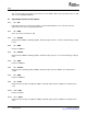
The EVM comes from the factory with the following default settings on the jumpers.
Table 1. Jumper Settings
Jumper Shunt Location
JP1 Between V-Hi and DEF1
JP2 Between V-Hi and DEF2
JP3 Between ON and DCDC1
JP4 Between ON and DCDC2
JP5 Between V-Hi and DEF3
JP6 Between ON and DCDC3
JP7 Between PWM and MODE
JP8 Between ON and LDO
JP9 Between ON and VDD_ALIVE
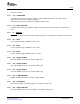
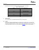
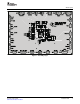
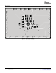
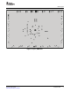
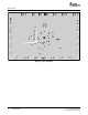
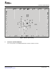
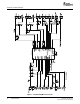
This section provides the TPS650241EVM-234 board layout and illustrations.
Board layout is critical for all switch mode power supplies. Figure 1 through Figure 5 shows the board
layout for the TPS650241EVM-234 PWB. The nodes with high switching frequencies and currents are
short and are isolated from the noise sensitive feedback circuitry. Careful attention has been given to the
routing of high frequency current loops. See the data sheet (SLVS774 ) for specific layout guidelines.
4 TPS650241EVM SLVU218 – August 2007
Submit Documentation Feedback