TPS65140EVMĆ031 User’s Guide February 2004 PMP Portable Power SLVU104
IMPORTANT NOTICE Texas Instruments Incorporated and its subsidiaries (TI) reserve the right to make corrections, modifications, enhancements, improvements, and other changes to its products and services at any time and to discontinue any product or service without notice. Customers should obtain the latest relevant information before placing orders and should verify that such information is current and complete.
EVM IMPORTANT NOTICE Texas Instruments (TI) provides the enclosed product(s) under the following conditions: This evaluation kit being sold by TI is intended for use for ENGINEERING DEVELOPMENT OR EVALUATION PURPOSES ONLY and is not considered by TI to be fit for commercial use.
EVM WARNINGS AND RESTRICTIONS It is important to operate this EVM within the input voltage range of 2.7 V to 5.8 V. Exceeding the specified input range may cause unexpected operation and/or irreversible damage to the EVM. If there are questions concerning the input range, please contact a TI field representative prior to connecting the input power. Applying loads outside of the specified output range may result in unintended operation and/or possible permanent damage to the EVM.
Preface About This Manual This users guide describes the characteristics, operation, and use of the TPS65140EVM-031 evaluation module (EVM). This EVM contains Texas Instruments TPS65140 triple output LCD supply IC with linear regulator controller and VCOM buffer. This users guide includes EVM specifications, test results, schematic diagram, bill of materials (BOM), and recommended test setup.
-4
1 Introduction . . . . . . . . . . . . . . . . . . . . . . . . . . . . . . . . . . . . . . . . . . . . . . . . . . . . . . . . . . . . . . . . . . . . . 1.1 Background . . . . . . . . . . . . . . . . . . . . . . . . . . . . . . . . . . . . . . . . . . . . . . . . . . . . . . . . . . . . . . . . 1.2 Performance Specification Summary . . . . . . . . . . . . . . . . . . . . . . . . . . . . . . . . . . . . . . . . . . 1.3 Modifications . . . . . . . . . . . . . . . . . . . . . . . . . . . . . . . . . . .
2−1 2−2 2−3 3−1 3−2 3−3 4−1 TPS65140 VOUT1 Efficiency . . . . . . . . . . . . . . . . . . . . . . . . . . . . . . . . . . . . . . . . . . . . . . . . . . . TPS65140 Main Boost Converter Load Transient for VI = 3.3 V and VO = 10 V . . . . . . . . TPS65140 Main Boost Converter Load Transient for VI = 5 V and VO = 13.5 V . . . . . . . . Top Assembly Layer . . . . . . . . . . . . . . . . . . . . . . . . . . . . . . . . . . . . . . . . . . . . . . . . . . . . . . . . . . . Top Layer Routing . . . . . . .
Chapter 1 This chapter contains background information for the TPS65140EVM-031 evaluation module. Topic Page 1.1 Background . . . . . . . . . . . . . . . . . . . . . . . . . . . . . . . . . . . . . . . . . . . . . . . . . . 1-2 1.2 Performance Specification Summary . . . . . . . . . . . . . . . . . . . . . . . . . . . 1-2 1.3 Modifications . . . . . . . . . . . . . . . . . . . . . . . . . . . . . . . . . . . . . . . . . . . . . . . . .
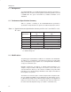
Background 1.1 Background The TPS65140EVM uses a TPS65140 multichannel output IC to provide three LCD power rails, as well as a linear regulator controller to provide 3.3 V and a VCOM buffer. The goal of the EVM is to facilitate evaluation of the TPS65140. 1.2 Performance Specification Summary Table 1−1 provides a summary of the TPS65140EVM−031 performance specifications. All specifications are given for an ambient temperature of 25°C. Table 1−1. Typical Performance Specification Summary for VIN = 3.
Modifications Table 1−2. Typical Performance Specification Summary for VIN = 5 V and VOUT1 = 13.5V, TA = 255C Voltage Range (V) Specification Min VIN Typ Current Range (mA) Max Min Typ Max 4.0 5 5.8 2000 VOUT1 13.30 13.5 13.70 0 VOUT2 −7.11 −7 −6.86 0 20 (1) VOUT3 22.5 23 23.5 0 20 (1) VOUT4 3.2 3.3 3.4 0 500 (1) VCOM 6.65 6.75 6.85 0 650 peak (1) 400 1) Maximum currents are determined by ambient conditions.
Modifications (This page has been left blank intentionally.
Chapter 2 This chapter describes how to properly test the TPS65140 using the TPS65140EVM−031. Topic Page 2.1 Input/Output Connect . . . . . . . . . . . . . . . . . . . . . . . . . . . . . . . . . . . . . . . . . 2-2 2.2 Test Setup . . . . . . . . . . . . . . . . . . . . . . . . . . . . . . . . . . . . . . . . . . . . . . . . . . . . 2-3 2.3 Test Results . . . . . . . . . . . . . . . . . . . . . . . . . . . . . . . . . . . . . . . . . . . . . . . . . .
Input/Output Connect 2.1 Input/Output Connect The EVM connection points are described in the following paragraphs. 2.1.1 J1−VIN This is the positive connection to the input power supply. The leads to the input supply should be twisted and kept as short as possible. 2.1.2 J2−GND This is the return connection to the input power supply. 2.1.3 J3−VOUT1 This is the positive output for the main boost convertr of the device. 2.1.
Test Setup 2.1.13 JP1 − Mode This is the charge pump mode pin connector. In order for the charge pump to operate as a voltage doubler, a jumper is installed to pull the mode pin to GND and C16 is left unpopulated. In order for the charge pump to operate as a voltage tripler, the jumper is removed and C16 is populated. 2.1.14 JP2−Enable (EN) This is the enable pin for the main boost converter (VOUT1). The enable pin is pulled up to Vin by an onboard pullup resistor.
Test Results Figure 2−2. TPS65140 Main Boost Converter Load Transient for VIN = 3.3V and VOUT = 10V Figure 2−3. TPS65140 Main Boost Converter Load Transient for VIN = 5 V and VOUT = 13.
Chapter 3 This chapter provides the TPS65140EVM−031 board layout and illustrations. Topic 3.1 Page Layout . . . . . . . . . . . . . . . . . . . . . . . . . . . . . . . . . . . . . . . . . . . . . . . . . . . . . . .
Layout 3.1 Layout Board layout is critical for all switch mode power supplies. Figures 3−1, 3−2, and 3−3 show the board layout for the HPA030 PWB. The switching nodes with high frequency noise are isolated from the noise sensitive feedback circuitry and careful attention has been given to the routing of high frequency current loops. Refer to the data sheet for more specific layout guidelines. Figure 3−1. Top Assembly Layer Figure 3−2.
Layout Figure 3−3.
Layout (This page has been left blank intentionally.
Chapter 4 ! This chapter provides the TPS65140EVM-031 bill of materials and schematic. Topic Page 4.1 Bill of Materials . . . . . . . . . . . . . . . . . . . . . . . . . . . . . . . . . . . . . . . . . . . . . . . 4-2 4.2 Schematic . . . . . . . . . . . . . . . . . . . . . . . . . . . . . . . . . . . . . . . . . . . . . . . . . . . .
Table 4−1. Bill of Materials for VIN = 3.3 V and VOUT1 = 10 V Count Ref Des Description Size MFR Part Number 1 C1 Capacitor, ceramic, 22−µF, 16−V, X5R, 10% 1210 TDK C3225X5R1C226KT 1 C10 Capacitor, ceramic, 1.0−µF, 10−V, X5R, 10% 603 TDK C1608X5R1A105KT 0 C11 Capacitor, ceramic, xxx−µF, vv−V 603 1 C13 Capacitor, ceramic, 0.22−µF, 50−V, X5R, 20% 805 TDK C2012X5R1H224KT 1 C14 Capacitor, ceramic, 4.7−µF, 6.
Table 4−2. Bill of Materials for VIN = 5.0 V and VOUT1 = 13.5 V Count Ref Des Description Size MFR Part Number 1 C1 Capacitor, ceramic, 22−µF, 16−V, X5R, 10% 1210 TDK C3225X5R1C226KT 1 C10 Capacitor, ceramic, 1.0−µF, 10−V, X5R, 10% 603 TDK C1608X5R1A105KT 0 C11 Capacitor, ceramic, xxx−µF, vv−V 603 1 C13 Capacitor, ceramic, 0.22−µF, 50−V, X5R, 20% 805 TDK C2012X5R1H224KT 1 C14 Capacitor, ceramic, 4.7−µF, 6.
Schematic 4.1 Schematic Figure 4−1. TPS65140EVM−031 Schematic for VIN = 3.3 V and VOUT1 = 10 V.
Schematic (This page has been left blank intentionally.