TPS65720 TPS65721 www.ti.com SLVS979 – OCTOBER 2009 PMU for Bluetooth Headsets Check for Samples: TPS65720 TPS65721 FEATURES 1 • • 2 • • • • • • • • • • • • • • Battery Charger With Power Path Management 28 V Rated Power Path With: – 100 mA Input Current Limit – 500 mA input Current Limit 300 mA Charge Current 200 mA Step-Down Converter for TPS65720 400 mA Step-Down Converter for TPS65721 Up to 92% Efficiency VIN Range for DCDC Converter From 2.3V to 5.6V 2.
TPS65720 TPS65721 SLVS979 – OCTOBER 2009 www.ti.com This integrated circuit can be damaged by ESD. Texas Instruments recommends that all integrated circuits be handled with appropriate precautions. Failure to observe proper handling and installation procedures can cause damage. ESD damage can range from subtle performance degradation to complete device failure.
TPS65720 TPS65721 www.ti.com SLVS979 – OCTOBER 2009 RECOMMENDED OPERATING CONDITIONS (continued) MIN NOM MAX UNIT CINAC Input capacitor at AC (1) 0.1 1 μF CBAT Capacitor at BAT (1) 0.1 4.7 μF CSYS Capacitor at SYS (1) 4.7 10 μF (1) 4.7 μF CINDCDC1 Input capacitor at VINDCDC1 SYS and CINDCDC1 COUTDCDC1 Output capacitor at VDCDC1 (1) 4.7 CINLDO1 Input capacitor at VINLDO1 (1) 2.2 μF COUTLDO1 Output capacitor at LDO1 (1) 2.
TPS65720 TPS65721 SLVS979 – OCTOBER 2009 www.ti.com ELECTRICAL CHARACTERISTICS (continued) VSYS = 3.6V, VDCDC1 = 2.05V, PFM mode, L = 3.3μH, COUTDCDC1 = 4.7μF, VINLDO1=2.05V, VLDO1=1.
TPS65720 TPS65721 www.ti.com SLVS979 – OCTOBER 2009 ELECTRICAL CHARACTERISTICS (continued) VSYS = 3.6V, VDCDC1 = 2.05V, PFM mode, L = 3.3μH, COUTDCDC1 = 4.7μF, VINLDO1=2.05V, VLDO1=1.
TPS65720 TPS65721 SLVS979 – OCTOBER 2009 www.ti.com ELECTRICAL CHARACTERISTICS (continued) VSYS = 3.6V, VDCDC1 = 2.05V, PFM mode, L = 3.3μH, COUTDCDC1 = 4.7μF, VINLDO1=2.05V, VLDO1=1.
TPS65720 TPS65721 www.ti.com SLVS979 – OCTOBER 2009 ELECTRICAL CHARACTERISTICS (continued) VSYS = 3.6V, VDCDC1 = 2.05V, PFM mode, L = 3.3μH, COUTDCDC1 = 4.7μF, VINLDO1=2.05V, VLDO1=1.85V, TA = –40°C to 85°C typical values apply in a temperature range of 10°C to 35°C (unless otherwise noted) PARAMETER ITERM TEST CONDITIONS Charge current value for termination detection threshold (internally set) MIN TYP MAX for I_TERM[1,0]=11 (termination current is 20% of charge current) 0.15×ICHG 0.2×ICHG 0.
TPS65720 TPS65721 SLVS979 – OCTOBER 2009 www.ti.com ELECTRICAL CHARACTERISTICS (continued) VSYS = 3.6V, VDCDC1 = 2.05V, PFM mode, L = 3.3μH, COUTDCDC1 = 4.7μF, VINLDO1=2.05V, VLDO1=1.85V, TA = –40°C to 85°C typical values apply in a temperature range of 10°C to 35°C (unless otherwise noted) PARAMETER TEST CONDITIONS MIN TYP MAX UNIT Thermistor high temperature detection resistance (equals 45°C for 10k NTC; B=3380) 4.3 5 5.
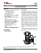
TPS65720 TPS65721 www.ti.com SLVS979 – OCTOBER 2009 DEVICE INFORMATION Chip scale version (YFF package): PIN ASSIGNMENT (bottom view) AC ISET RESET SDAT SCLK A5 SYS SYS PB_IN GPIO0 GPIO1 A4 BAT BAT GPIO2 INT GPIO3 A3 HOLD_ DCDC1 L1 TS HOLD_ LDO1 GND A2 FB_ DCDC1 PGND E1 AGND D1 VINLDO1 C1 VLDO1 B1 A1 FUNCTIONAL BLOCK DIAGRAM TPS65720 BAT AC BAT 1uF charger / power path NTC SYS ISET set charge current LiIon TS SYS 4.7uF R5 L1 HOLD_DCDC1 DCDC1 200mA 2.
TPS65720 TPS65721 SLVS979 – OCTOBER 2009 www.ti.com PIN FUNCTIONS for CHIP SCALE VERSION (YFF package) PIN NAME NO. I/O DESCRIPTION AC E5 I Input power for power manager, connect to external DC supply. SYS E4, D4 O System voltage; output of the power path manager.
TPS65720 TPS65721 www.ti.com SLVS979 – OCTOBER 2009 FUNCTIONAL BLOCK DIAGRAM TPS65721 AC BAT AC BAT 1uF NTC SYS ISET set charge current LiIon TS charger / power path SYS 4.7uF R5 L1 MODE DCDC 1 200mA HOLD_DCDC1 2.2uH 4.7uF Vout1 R1 FB_DCDC1 22pF R2 VINLDO1 VLDO1 LDO1 200 mA HOLD_LDO1 Vout2 R3 2.
TPS65720 TPS65721 SLVS979 – OCTOBER 2009 www.ti.com PIN FUNCTIONS for QFN VERSION (RSN package) (continued) PIN NAME NO. I/O DESCRIPTION RESET 14 O Open drain output of the reset generator; This output goes active LOW when the input voltage at pin THRESHOLD falls below the threshold voltage. THRESHOLD 3 I Input voltage to the reset comparator. When the input voltage falls below the threshold, the RESET output is actively pulled LOW.
TPS65720 TPS65721 www.ti.com SLVS979 – OCTOBER 2009 TYPICAL CHARACTERISTICS (continued) FIGURE Output voltage ripple in PWM mode; DCDC1 Scope plot: Vi = 3.6V Vo = 2.05V; Io = 60mA (PWM) Figure 14 Startup DCDC1 and LDO1 Scope plot using TPS65720 (battery powered) for /PB_IN; Vo_DCDC1; Vo_LDO1 Figure 15 Load transient response LDO1 Scope plot; V = 1.85V; Vi = 2.05V I = 50 μA to 60mA to 50 μA Figure 16 Line transient response LDO1 Scope plot; Vo = 1.85V; Vi = 5V to 3.
TPS65720 TPS65721 SLVS979 – OCTOBER 2009 www.ti.com TPS65721 Efficiency of DCDC1 vs Load Current; PWM Mode; inductor: MIPSA2520 2.2uH TPS65721 Efficiency of DCDC1 vs Load Current; PFM Mode; inductor: MIPSA2520 2.2uH 100 100 VO = 3.3 V VO = 3.3 V 90 90 80 VI = 3.4 V 80 VI = 3.4 V VI = 3.6 V 70 Efficiency - % Efficiency - % 70 VI = 3.6 V 60 50 VI = 4.2 V 40 VI = 5 V 50 30 20 20 10 10 0.0001 0.01 0.001 IO - Output Current - A 0.1 VI = 5 V 40 30 0 0.00001 VI = 4.2 V 60 0 0.
TPS65720 TPS65721 www.ti.com SLVS979 – OCTOBER 2009 Load Transient Response PWM Mode VI = 3.6 V Line Transient Response PWM Mode IO = 60 mA VI = 3.6 V to 5 V to 3.6 V IO = 40 mA to 360 mA VO = 3.3 V VO = 2.05 V Time - 100 ms/div Time - 100 ms/div Figure 11. Figure 12. Output Voltage Ripple on DCDC1 PFM Mode Output Voltage Ripple on DCDC1 PWM Mode VI = 3.6 V, PWM IO = 60 mA VI = 3.6 V, PFM IO = 50 mA VO = 2.05 V VO = 2.05 V 20 mV/div 20 mV/div Time - 1 ms/div Time - 2 ms/div Figure 13.
TPS65720 TPS65721 SLVS979 – OCTOBER 2009 www.ti.com Kset vs Riset Line Transient Response LDO1 150 IO = 60 mA 145 TA = 25°C VI = 5 V to 3.6 V to 5 V 140 KISET - AW 135 TA = -40°C TA = 85°C 130 125 VO = 1.85 V 120 115 110 Time - 100 ms/div 0 4000 8000 12000 RISET - W 16000 Figure 17. Figure 18.
TPS65720 TPS65721 www.ti.com SLVS979 – OCTOBER 2009 Kset vs Riset Efficiency vs output current for the complete system; LDO1 powered by DCDC1 with VDCDC1=2.05V; VLDO1= 1.85V 505 100 500 90 TA = -40°C 495 VI = 3 V VI = 3.6 V 80 70 485 Efficiency - % KISET - AW VI = 4.2 V TA = 25°C 490 TA = 85°C 480 VI = 2.5 V 60 VI = 5 V 50 40 475 30 470 20 465 10 460 0 4000 8000 12000 RISET - W 16000 20000 24000 0 0.00001 0.0001 Figure 21. ICH_SCL[1,0]=11 0.01 0.
TPS65720 TPS65721 SLVS979 – OCTOBER 2009 www.ti.com POWER-ON RESET MODE The charger enters power-on reset mode when the input voltage at AC is within the valid range: VAC > UVLO and VAC > VBAT + VIN(DT) and VAC < VOVP, and the Bits indicate that the USB suspend mode is not enabled [≠ (0,0)]. During power-on reset mode, all internal timers and other circuit blocks are activated.
TPS65720 TPS65721 www.ti.
TPS65720 TPS65721 SLVS979 – OCTOBER 2009 www.ti.com CC FAST CHARGE PRECHARGE CV TAPER DONE VBAT(REG) IO(CHG) Battery Current Battery Voltage VLOWV TERM CURRENT = 1 I(PRECHG) I(TERM) Figure 24. Battery Charge In the precharge phase, the battery is charged with the precharge current (IPRECHG). Once the battery voltage crosses the VLOWV threshold, the battery is charged with the fast-charge current (ICHG).
TPS65720 TPS65721 www.ti.com SLVS979 – OCTOBER 2009 If the BAT voltage falls below VLOWV during the battery detection test, it indicates that the battery has been removed. The device then checks for battery insertion. The FET Q2 is turned on and sources IPRECHG out of BAT for the duration of tDET. If the battery voltage does not rise above VRCH, it indicates that a battery has been inserted, and a new charge cycle begins.
TPS65720 TPS65721 SLVS979 – OCTOBER 2009 www.ti.com PRECHARGE THERMAL REGULATION CC FAST CHARGE CV TAPER DONE VO(REG) IO(CHG) Battery Voltage Battery Current V(LOWV) TERM CURRENT = 1 I(PRECHG) I(TERM) IC junction temperature, Tj TJ(REG) Figure 25. Thermal Loop TIMER FAULT If the pre-charge timer expires before the battery voltage reaches VLOWV, the charger indicates a fault condition.
TPS65720 TPS65721 www.ti.com SLVS979 – OCTOBER 2009 window, charging is resumed and the timers continue counting. When charging is suspended due to a battery pack temperature fault, the CH_ACTIVE Bit remains 1 and continues to indicate charging. Battery pack temperature sensing is disabled when termination is disabled () and the voltage at TS is greater than VDIS(TS). The battery pack temperature monitoring is disabled by connecting a 10-kΩ resistor from TS to GND.
TPS65720 TPS65721 SLVS979 – OCTOBER 2009 www.ti.com Dynamic Voltage Positioning This feature reduces the voltage under/overshoots at load steps from light to heavy load and vice versa. It is active in Power Save Mode and regulates the output voltage 1% higher than the nominal value. This provides more headroom for both the voltage drop at a load step, and the voltage increase at a load throw-off.
TPS65720 TPS65721 www.ti.com SLVS979 – OCTOBER 2009 Under-Voltage Lockout The under voltage lockout circuit prevents the device from malfunctioning at low input voltages and from excessive discharge of the battery and disables the converters and LDOs. The under-voltage lockout threshold is typically 2.2V. SHORT-CIRCUIT PROTECTION All outputs are short circuit protected with a maximum output current as defined in the electrical specifications.
TPS65720 TPS65721 SLVS979 – OCTOBER 2009 www.ti.com There is a power-hold pin for DCDC1 (HOLD_DCDC1) and one for LDO1 (HOLD_LDO1). When HOLD_DCDC1 is pulled HIGH, DCDC1 is kept enabled after PB_IN was released HIGH. HOLD_LDO1 serves the same function and keeps LDO1 enabled after PB_IN was released HIGH.
TPS65720 TPS65721 www.ti.com SLVS979 – OCTOBER 2009 INT Output Actively low, open drain interrupt output. Connect external pull-up resistor. Interrupts are flagged in the registers IR0, IR1 and IR2 if the interrupt is not masked by registers IRMASK0, IRMASK1 and IRMASK2. Per default, all interrupts are masked. Interrupts which are unmasked will set the Bit in either on the rising edge or on both edges. Details can be found in the register description for IR0, IR1 and IR2.
TPS65720 TPS65721 SLVS979 – OCTOBER 2009 www.ti.com ... SCLK SDAT A6 A5 ... A4 ... A0 R/W ACK 0 Start R7 R6 ... ... R5 R0 ACK 0 D7 D6 D5 ... D0 ACK 0 Slave Address 0 Register Address Stop Data NOTE: SLAVE =TPS65720 Figure 30. Serial I/f WRITE to TPS65720 Device ... SCLK SDAT A6 .. ... R/W ACK A0 0 .. R7 ... ... R0 ACK 0 ..
TPS65720 TPS65721 www.ti.
TPS65720 TPS65721 SLVS979 – OCTOBER 2009 www.ti.com CHGSTATUS Register Address: 01h (read only) CHGSTATUS Bit name and function Default B7 B6 B5 TS_HOT TS_COLD OVP x x x R R R B4 B3 B2 B1 CH_ACTIVE CH_PGOOD CH_THLOOP BO 0 x x x 0 R R R R R Default value loaded by: Read/write Bit 7 TS_HOT: 0 = battery temperature is below high temperature threshold (45°C/50°C/55°C/60°C). 1 = battery temperature is above high temperature threshold (45°C/50°C/55°C/60°C).
TPS65720 TPS65721 www.ti.com SLVS979 – OCTOBER 2009 CHGCONFIG0 Register Address: 02h (read/write) CHGCONFIG0 Bit name and function B7 B6 B5 B4 B3 B2 B1 BO VSYS1 VSYS0 AC input current1 AC input current0 TH_LOOP DYN_TMR TERM_EN CH_EN 0 1 1 0 1 1 0 0 1 1 1 1 1 1 1 1 UVLO/R UVLO/R UVLO/R UVLO/R UVLO/R UVLO/R UVLO/R UVLO/R R/W R/W R/W R/W R/W R/W R/W R/W Default For TPS65720 For TPS65721 Default value loaded by: Read/write Bit 7..6 VSYS1..
TPS65720 TPS65721 SLVS979 – OCTOBER 2009 www.ti.com CHGCONFIG1 Register Address: 03h (read/write) CHGCONFIG1 Bit name and function Default For TPS65720 For TPS65721 Default value loaded by: Read/write B7 B6 B5 B4 B3 B2 I_PRE1 I_PRE0 ICH_SCL1 ICH_SCL0 I_TERM1 I_TERM0 0 0 1 1 0 1 1 1 0 0 1 1 UVLO/R UVLO/R UVLO/R UVLO/R UVLO/R UVLO/R R/W R/W R/W R/W R/W R/W B1 BO 0 1 0 1 R R Bit 7..6 I_PRE1..
TPS65720 TPS65721 www.ti.com SLVS979 – OCTOBER 2009 CHGCONFIG2 Register Address: 04h (read/write) CHGCONFIG2 Bit name and function Default Default value loaded by: Read/write B7 B6 B5 SFTY_TMR1 0 SFTY_TMR PRE_TMR 0 1 0 UVLO/R UVLO/R UVLO/R R/W R/W R/W B4 0 R B3 B2 B1 NTC V_DPPM VBAT_COMP_EN 1 1 0 UVLO/R UVLO/R UVLO/R R/W R/W R/W Bit 7..6 SFTY_TMR1..
TPS65720 TPS65721 SLVS979 – OCTOBER 2009 www.ti.com CHGCONFIG3 Register Address: 05h (read/write) CHGCONFIG3 Bit name and function Default Default value loaded by: Read/write B7 B6 B5 B4 B3 B2 B1 BO CH_VLTG2 CH_VLTG1 CH_VLTG0 TMP_SHIFT1 TMP_SHIFT0 VBAT1 VBAT0 VBAT_COMP 0 1 0 0 0 0 0 1 UVLO/R UVLO/R UVLO/R UVLO/R UVLO/R UVLO/R UVLO/R UVLO/R R/W R/W R/W R/W R/W R/W R/W R Bit 7..5 CH_VLTG2..CH_VLTG0 (charge voltage selection): 000 = 4.15V 001 = 4.175V 010 = 4.
TPS65720 TPS65721 www.ti.
TPS65720 TPS65721 SLVS979 – OCTOBER 2009 www.ti.
TPS65720 TPS65721 www.ti.com SLVS979 – OCTOBER 2009 OUTPUT VOLTAGE [V] B5 B4 B3 B2 B1 B0 25 1.425 0 1 1 0 0 1 26 1.450 0 1 1 0 1 0 27 1.475 0 1 1 0 1 1 28 1.500 0 1 1 1 0 0 29 1.525 0 1 1 1 0 1 30 1.550 0 1 1 1 1 0 31 1.575 0 1 1 1 1 1 32 1.600 1 0 0 0 0 0 33 1.650 1 0 0 0 0 1 34 1.700 1 0 0 0 1 0 35 1.750 1 0 0 0 1 1 36 1.800 1 0 0 1 0 0 37 1.850 1 0 0 1 0 1 38 1.900 1 0 0 1 1 0 39 1.
TPS65720 TPS65721 SLVS979 – OCTOBER 2009 www.ti.
TPS65720 TPS65721 www.ti.
TPS65720 TPS65721 SLVS979 – OCTOBER 2009 www.ti.
TPS65720 TPS65721 www.ti.com SLVS979 – OCTOBER 2009 IRMASK1 Register Address: 0Eh (read/write) IRMASK1 Bit name and function B7 B6 B5 B4 B3 B2 B1 BO M_CH_ SLEEP M_CH_ RESET M_CH_IDLE M_CH_PRECH M_CH_ CC M_CH_ LDO M_CH_ FAULT M_CH_ SUSP Default Default value loaded by: Read/write Bit 7..
TPS65720 TPS65721 SLVS979 – OCTOBER 2009 www.ti.com IR1 Register Address: 11h (read) IR1 Bit name and function Default Default value loaded by: Set by: Read/write Bit 7..
TPS65720 TPS65721 www.ti.com SLVS979 – OCTOBER 2009 APPLICATION INFORMATION OUTPUT VOLTAGE SETTING DCDC1 The output voltage of the DCDC converter can be set with external resistor network on Pin FB_DCDC1. The feedback voltage is 0.6V. It is recommended to set the total resistance of R1 + R2 to less than 1MΩ. Route the FB_DCDC1 trace separate from noise sources, such as the inductor trace (L1). VFB-DCDC1 = 0.
TPS65720 TPS65721 SLVS979 – OCTOBER 2009 www.ti.com OUTPUT FILTER DESIGN (INDUCTOR AND OUTPUT CAPACITOR) Inductor Selection The converter operates typically with 3.3μH output inductor. Larger or smaller inductor values can be used to optimize the performance of the device for specific operation conditions. The selected inductor has to be rated for its DC resistance and saturation current. The DC resistance of the inductance will influence directly the efficiency of the converter.
TPS65720 TPS65721 www.ti.com SLVS979 – OCTOBER 2009 Vout ö 1 Vin ´ æ + ESR ÷ ç L ´ ¦ è 8 ´ Cout ´ ¦ ø 1DVout = Vout ´ (5) Where the highest output voltage ripple occurs at the highest input voltage Vin. At light load currents the converter operates in Power Save Mode and the output voltage ripple is dependent on the output capacitor value. The output voltage ripple is set by the internal comparator delay and the external capacitor.
TPS65720 TPS65721 SLVS979 – OCTOBER 2009 www.ti.com above a certain limit. In TPS6572x, the voltage at the output of the power path (SYS) is regulated to what is defined with VSYS[1,0] in register CHCONFIG0. When the current needed for the load and for charging the battery exceeds the input current limit, the voltage at SYS will collapse. The DPPM loop will reduce the charge current, such that the total current for the load and the charge current equals the input current limit.
TPS65720 TPS65721 www.ti.com SLVS979 – OCTOBER 2009 APPLICATION CIRCUITS TPS65720 BAT AC BAT 1uF charger / power path LiIon NTC SYS ISET 3k for a charge current of 150mA 10k TS SYS 4.7uF / 6.3V R5 L1 DCDC 1 200 mA 2.2uH VDCDC 1=2.05 V R1 360 k 4.7uF 22pF FB_DCDC1 R2 150k bluetooth chip VINLDO1 2.2uF LDO1 200 mA VLDO 1 = 1.85V VLDO1 4.7uF / 4V 2 x 3.
PACKAGE OPTION ADDENDUM www.ti.
PACKAGE OPTION ADDENDUM www.ti.
PACKAGE MATERIALS INFORMATION www.ti.com 1-Oct-2013 TAPE AND REEL INFORMATION *All dimensions are nominal Device Package Package Pins Type Drawing SPQ TPS65720YFFR DSBGA 3000 180.0 YFF 25 Reel Reel A0 Diameter Width (mm) (mm) W1 (mm) 8.4 2.38 B0 (mm) K0 (mm) P1 (mm) 2.4 0.8 4.0 W Pin1 (mm) Quadrant 8.0 Q1 TPS65720YFFT DSBGA YFF 25 250 180.0 8.4 2.38 2.4 0.8 4.0 8.0 Q1 TPS65721RSNR QFN RSN 32 3000 330.0 12.4 4.25 4.25 1.15 8.0 12.
PACKAGE MATERIALS INFORMATION www.ti.com 1-Oct-2013 *All dimensions are nominal Device Package Type Package Drawing Pins SPQ Length (mm) Width (mm) Height (mm) TPS65720YFFR DSBGA YFF 25 3000 182.0 182.0 17.0 TPS65720YFFT DSBGA YFF 25 250 182.0 182.0 17.0 TPS65721RSNR QFN RSN 32 3000 367.0 367.0 35.0 TPS65721RSNT QFN RSN 32 250 210.0 185.0 35.
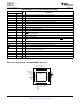
D: Max = 2.116 mm, Min =2.056 mm E: Max = 2.116 mm, Min =2.
IMPORTANT NOTICE Texas Instruments Incorporated and its subsidiaries (TI) reserve the right to make corrections, enhancements, improvements and other changes to its semiconductor products and services per JESD46, latest issue, and to discontinue any product or service per JESD48, latest issue. Buyers should obtain the latest relevant information before placing orders and should verify that such information is current and complete.