TPS65820 www.ti.com ..............................................................................................................................................................
TPS65820 SLVS663B – MAY 2006 – REVISED APRIL 2008 .............................................................................................................................................................. www.ti.com This integrated circuit can be damaged by ESD. Texas Instruments recommends that all integrated circuits be handled with appropriate precautions. Failure to observe proper handling and installation procedures can cause damage.
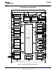
TPS65820 www.ti.com .............................................................................................................................................................. SLVS663B – MAY 2006 – REVISED APRIL 2008 FUNCTIONAL BLOCK DIAGRAM TPS65820 AC OUT OUT USB BAT LDO_PM LDO_PM 3.3V 10 mA AGND1 OUT 1.8V/3V 8 mA OUT RTC_OUT BAT BAT ON/OFF SIM,RTC LDOS SIM OUT POWER PATH CONTROL LINEAR CHARGER SYSTEM POWER CHARGE MANAGEMENT AGND1 TS DPPM TMR ISET1 OUT AGND1 2.6V/3.
TPS65820 SLVS663B – MAY 2006 – REVISED APRIL 2008 .............................................................................................................................................................. www.ti.com ABSOLUTE MAXIMUM RATINGS over operating free-air temperature range (unless otherwise noted) (1) VALUE AC and USB with respect to AGND1 ANLG1, ANLG2 with respect to AGND2 –0.3 to V(OUT) V(OUT) with respect to AGND1 5 VIN_LDO12, VIN_LDO35, LDO3, LDO4, LDO5 with respect to AGND2 –0.
TPS65820 www.ti.com .............................................................................................................................................................. SLVS663B – MAY 2006 – REVISED APRIL 2008 RECOMMENDED OPERATING CONDITIONS MIN MAX 4.35 (1) V 0 2.6 V Greater of : 3.6 V OR minimum input voltage required for LDO/converter operation outside dropout region 4.
TPS65820 SLVS663B – MAY 2006 – REVISED APRIL 2008 .............................................................................................................................................................. www.ti.
TPS65820 www.ti.com .............................................................................................................................................................. SLVS663B – MAY 2006 – REVISED APRIL 2008 ELECTRICAL CHARACTERISTICS – SYSTEM SEQUENCING AND OPERATING MODES Over recommended operating conditions (typical values at TJ = 25°C), application circuit as in Figure 3 (unless otherwise noted).
TPS65820 SLVS663B – MAY 2006 – REVISED APRIL 2008 .............................................................................................................................................................. www.ti.com ELECTRICAL CHARACTERISTICS – POWER PATH AND CHARGE MANAGEMENT Over recommended operating conditions (typical values at TJ = 25°C), application circuit as in Figure 3 (unless otherwise noted).
TPS65820 www.ti.com .............................................................................................................................................................. SLVS663B – MAY 2006 – REVISED APRIL 2008 ELECTRICAL CHARACTERISTICS – POWER PATH AND CHARGE MANAGEMENT (Continued) Over recommended operating conditions (typical values at TJ = 25°C), application circuit as in Figure 3 (unless otherwise noted).
TPS65820 SLVS663B – MAY 2006 – REVISED APRIL 2008 .............................................................................................................................................................. www.ti.com ELECTRICAL CHARACTERISTICS – POWER PATH AND CHARGE MANAGEMENT (Continued) Over recommended operating conditions (typical values at TJ = 25°C), application circuit as in Figure 3 (unless otherwise noted).
TPS65820 www.ti.com .............................................................................................................................................................. SLVS663B – MAY 2006 – REVISED APRIL 2008 ELECTRICAL CHARACTERISTICS – LINEAR REGULATORS Over recommended operating conditions (typical values at TJ = 25°C), application circuit as in Figure 3 (unless otherwise noted).
TPS65820 SLVS663B – MAY 2006 – REVISED APRIL 2008 .............................................................................................................................................................. www.ti.com ELECTRICAL CHARACTERISTICS – LINEAR REGULATORS (continued) Over recommended operating conditions (typical values at TJ = 25°C), application circuit as in Figure 3 (unless otherwise noted).
TPS65820 www.ti.com .............................................................................................................................................................. SLVS663B – MAY 2006 – REVISED APRIL 2008 ELECTRICAL CHARACTERISTICS – SWITCHED MODE SM1 STEP-DOWN CONVERTER Over recommended operating conditions (typical values at TJ = 25°C), VO(SM1) = 1.24 V, application circuit as in Figure 3 (unless otherwise noted).
TPS65820 SLVS663B – MAY 2006 – REVISED APRIL 2008 .............................................................................................................................................................. www.ti.com ELECTRICAL CHARACTERISTICS – SWITCHED MODE SM2 STEP-DOWN CONVERTER Over recommended operating conditions (typical values at TJ = 25°C), VO(SM1) = 1.24 V, application circuit as in Figure 3 (unless otherwise noted).
TPS65820 www.ti.com .............................................................................................................................................................. SLVS663B – MAY 2006 – REVISED APRIL 2008 ELECTRICAL CHARACTERISTICS – ADC Over recommended operating conditions (typical values at TJ = 25°C), V(ADC_REF) =2.535v if external reference voltage is used,application circuit as in Figure 3 (unless otherwise noted).
TPS65820 SLVS663B – MAY 2006 – REVISED APRIL 2008 .............................................................................................................................................................. www.ti.com ELECTRICAL CHARACTERISTICS – ADC (continued) Over recommended operating conditions (typical values at TJ = 25°C), V(ADC_REF) =2.535v if external reference voltage is used,application circuit as in Figure 3 (unless otherwise noted).
TPS65820 www.ti.com ..............................................................................................................................................................
TPS65820 SLVS663B – MAY 2006 – REVISED APRIL 2008 .............................................................................................................................................................. www.ti.
TPS65820 www.ti.com ..............................................................................................................................................................
TPS65820 SLVS663B – MAY 2006 – REVISED APRIL 2008 .............................................................................................................................................................. www.ti.com APPLICATION DIAGRAM + VSIM VRTC_OUT VL DO_PM VLDO0 VLDO1 VLDO2 AC_DC ADAPTER OUTPUT - GND USB POWER + C1 10uF - 7 AC C2 10uF GND C4 C5 VOUT VOUT 6 USB C3 2.2uF Supercap TPS65820 OUT 9 5 SIM ISET1 11 4 RTC_OUT 1uF BAT 17 A1 C6 C7 1uF 1uF C8 4.7uF C9 4.
TPS65820 www.ti.com .............................................................................................................................................................. SLVS663B – MAY 2006 – REVISED APRIL 2008 TYPICAL CHARACTERISTICS – POWER PATH MANAGEMENT Measured with Application Circuit shown in Figure 3, unless otherwise noted SWITCHING FROM AC TO BATTERY ON AC REMOVAL SWITCHING FROM USB TO BATTERY ON AC REMOVAL USB = 5 V, BAT = 3.3 V AC = 5 V, BAT = 3.
TPS65820 SLVS663B – MAY 2006 – REVISED APRIL 2008 .............................................................................................................................................................. www.ti.com TYPICAL CHARACTERISTICS – LINEAR REGULATORS 0, 1, 2 Measured with Application Circuit shown in Figure 3, unless otherwise noted LOAD REGULATION vs JUNCTION TEMPERATURE LINE REGULATION vs JUNCTION TEMPERATURE -0.500 0.25 VIN_LDO02 = 3.65 V, Load = 10 mA to 150 mA, CO(LDO02) = 1 mF 0.
TPS65820 www.ti.com .............................................................................................................................................................. SLVS663B – MAY 2006 – REVISED APRIL 2008 TYPICAL CHARACTERISTICS – LINEAR REGULATORS 3, 4, 5 Measured with Application Circuit shown in Figure 3, unless otherwise noted LOAD REGULATION vs JUNCTION TEMPERATURE LINE REGULATION vs JUNCTION TEMPERATURE -0.010 -0.5 VIN_LDO 35 = 3 V, Load = 10 mA to 150 mA, CO(LDO 35) = 1 mF -0.
TPS65820 SLVS663B – MAY 2006 – REVISED APRIL 2008 .............................................................................................................................................................. www.ti.
TPS65820 www.ti.com .............................................................................................................................................................. SLVS663B – MAY 2006 – REVISED APRIL 2008 TYPICAL CHARACTERISTICS – DRIVERS Measured with Application Circuit shown in Figure 3, unless otherwise noted LINE TRANSIENT LOAD TRANSIENT VIN_SM2 VO(SM2) VO_SM2 AC = 5 V, VIN_SM2 = 3 V (DC) + 1 V (AC), VO(SM2) = 1.8 V, IO(SM2) = 100 mA, L = 3.
TPS65820 SLVS663B – MAY 2006 – REVISED APRIL 2008 .............................................................................................................................................................. www.ti.com SERIAL INTERFACE Overview The TPS65820 is compatible with a host-controlled environment, with internal parameters and status information accessible via an I2C interface.
TPS65820 www.ti.com .............................................................................................................................................................. SLVS663B – MAY 2006 – REVISED APRIL 2008 Table 2.
TPS65820 SLVS663B – MAY 2006 – REVISED APRIL 2008 .............................................................................................................................................................. www.ti.com The I2C write protocol is similar to the read, without the need for a repeated start and bus being set in write mode. In a WRITE it is not necessary to end each 1 byte WRITE command with a STOP, a START has the same effect (repeated start). SCLK SDAT ... A6 ... ..
TPS65820 www.ti.com .............................................................................................................................................................. SLVS663B – MAY 2006 – REVISED APRIL 2008 Valid Read Sequences The TPS65820 always ACKs its own address. S hA1 bqA Upon receiving hA1, TPS65820 starts at wherever the RAM address register is pointing. The START and the STOP both act as priority interrupts.
TPS65820 SLVS663B – MAY 2006 – REVISED APRIL 2008 .............................................................................................................................................................. www.ti.
TPS65820 www.ti.com ..............................................................................................................................................................
TPS65820 SLVS663B – MAY 2006 – REVISED APRIL 2008 .............................................................................................................................................................. www.ti.com INTERRUPT CONTROLLER AND SYSTEM SEQUENCING Overview The TPS65820 has two dedicated internal controllers that execute the host interface and system sequencing tasks: a sequencing controller and an interrupt controller.
TPS65820 www.ti.com .............................................................................................................................................................. SLVS663B – MAY 2006 – REVISED APRIL 2008 SYSTEM SEQUENCING AND TPS65820 OPERATING MODES The TPS65820 has a state machine that controls the device power up and power down sequencing.
TPS65820 SLVS663B – MAY 2006 – REVISED APRIL 2008 .............................................................................................................................................................. www.ti.com Table 3. Integrated Supply and Drivers Power-Up Defaults SUPPLY POWER-UP DEFAULT OTHER BLOCKS POWER-UP DEFAULT LDO0 OFF, 3.3 V POWER PATH INPUT TO SYSTEM LDO1 2.85V, ON PWM OFF LDO2 3.3 V, ON PWM_LED OFF LDO3 1.25 V, ON GPIO1 INPUT LDO4 2.
TPS65820 www.ti.com .............................................................................................................................................................. SLVS663B – MAY 2006 – REVISED APRIL 2008 Table 4. Startup Sequence EEPROM Byte (Factory-Programmable Only) Bit B7 Function B6 B5 Choose 1 of 8 sequences; see Table 5. B4 B3 B2 Choose 1 of 4 initial delays; see Table 5. B1 B0 Choose 1 of 8 secondary delays; see Table 5. Table 5.
TPS65820 SLVS663B – MAY 2006 – REVISED APRIL 2008 .............................................................................................................................................................. www.ti.
TPS65820 www.ti.com .............................................................................................................................................................. SLVS663B – MAY 2006 – REVISED APRIL 2008 The RESPWRON signal set to a high level is the proper signal to use as an indicator that the device has transitioned out of the reset state. During the power-up sequence the RESPWRON pin is asserted LOW until the RESET TIMER expires.
TPS65820 SLVS663B – MAY 2006 – REVISED APRIL 2008 .............................................................................................................................................................. www.ti.com 2. If SLEEP was set by a system low voltage detection, or I2C bit SLEEP_MODE, only with battery present: Input power must be connected, setting the TPS65820 in the ENABLE mode.
TPS65820 www.ti.com ..............................................................................................................................................................
TPS65820 SLVS663B – MAY 2006 – REVISED APRIL 2008 .............................................................................................................................................................. www.ti.com SYSTEM STATUS — I2C REGISTERS The I2C registers that have system status data are shown below. The HEX address for each register is shown by the register name, together with the R or W functionality for the register bits.
TPS65820 www.ti.com .............................................................................................................................................................. SLVS663B – MAY 2006 – REVISED APRIL 2008 INTERRUPT CONTROLLER – I2C REGISTERS The I2C registers that control an interrupt generation (INT: HI→LO) are shown below. The HEX address for each register is shown by the register name, together with the R or W functionality for the register bits.
TPS65820 SLVS663B – MAY 2006 – REVISED APRIL 2008 .............................................................................................................................................................. www.ti.com FUNCTIONALITY GUIDE — SYSTEM POWER AND CHARGE MANAGEMENT CHARGE MANAGEMENT Fast Charge (1) Charge Current Value Charge Current Scaling IO(BAT), Programmable, 1.
TPS65820 www.ti.com ..............................................................................................................................................................
TPS65820 SLVS663B – MAY 2006 – REVISED APRIL 2008 .............................................................................................................................................................. www.ti.com The TPS65820 regulates the voltage at the OUT pin to 4.6 V, when one of the external supplies connected to pins AC or USB is powering the OUT pin. The selected input (AC or USB pin) current is limited to a value defined by I2C register settings.
TPS65820 www.ti.com .............................................................................................................................................................. SLVS663B – MAY 2006 – REVISED APRIL 2008 Table 6 lists the system power detection conditions. VIN(DT), VOUTSH, VBATSH, VOVP are TPS65820 internal references, refer to the electrical characteristics for additional details. Table 6.
TPS65820 SLVS663B – MAY 2006 – REVISED APRIL 2008 .............................................................................................................................................................. www.ti.com System Voltage Regulation The system voltage is regulated to a fixed voltage when one of the input power supplies is connected to the system. The system voltage regulation is implemented by a control loop that modulates the selected switch Rds(on).
TPS65820 www.ti.com .............................................................................................................................................................. SLVS663B – MAY 2006 – REVISED APRIL 2008 An internal comparator with a fixed deglitch time, t DGL(NOBAT) monitors the ANLG1 pin voltage, if V(ANLG1) > V(OUT) – VNOBATID a battery removed condition is detected and an internal discharge switch is activated, connecting an internal resistor from BAT pin to AGND1.
TPS65820 SLVS663B – MAY 2006 – REVISED APRIL 2008 .............................................................................................................................................................. www.ti.
TPS65820 www.ti.com ..............................................................................................................................................................
TPS65820 SLVS663B – MAY 2006 – REVISED APRIL 2008 .............................................................................................................................................................. www.ti.com The ISET1 resistor always sets the maximum charge current, if the AC input is selected. When the USB input is selected, the maximum charge current is defined by the USB input current limit and the programmed charge current.
TPS65820 www.ti.com .............................................................................................................................................................. SLVS663B – MAY 2006 – REVISED APRIL 2008 Once termination is detected, a new charge cycle starts if the voltage on the BAT pin falls below the V(RCH) threshold.
TPS65820 SLVS663B – MAY 2006 – REVISED APRIL 2008 .............................................................................................................................................................. www.ti.com CHARGER OFF MODE The TPS65820 charger circuitry enters the low-power OFF mode if both AC and USB power are not detected. This feature prevents draining the battery during the absence of input supply.
TPS65820 www.ti.com .............................................................................................................................................................. SLVS663B – MAY 2006 – REVISED APRIL 2008 DYNAMIC TIMER FUNCTION The charge and precharge safety timers are programmed by the user to detect a fault condition if the charge cycle duration exceeds the total time expected under normal conditions.
TPS65820 SLVS663B – MAY 2006 – REVISED APRIL 2008 .............................................................................................................................................................. www.ti.
TPS65820 www.ti.com .............................................................................................................................................................. SLVS663B – MAY 2006 – REVISED APRIL 2008 FUNCTIONALITY GUIDE — LINEAR REGULATORS SELECTABLE OUTPUT VOLTAGE LDO Supply ON/OFF Control Output Discharge Switch LDO1 Yes, set via I2C LDO2 OUTPUT VOLTAGE (V), set via I2C IO Max (mA) Acc % Power Up Default 1.25/1.5/1.8/2.5/2.85/3/3.2/3.3 150 3 ON, 2.85 V 8 1.25/1.5/1.8/2.
TPS65820 SLVS663B – MAY 2006 – REVISED APRIL 2008 .............................................................................................................................................................. www.ti.
TPS65820 www.ti.com .............................................................................................................................................................. SLVS663B – MAY 2006 – REVISED APRIL 2008 Output Voltage Monitoring Internal power good comparators monitor the LDO outputs and detect when the output voltage is below 90% of the programmed value.
TPS65820 SLVS663B – MAY 2006 – REVISED APRIL 2008 .............................................................................................................................................................. www.ti.com Table 10. LDO 3–5 Programming Step Values 58 Step B6–B0 Vset Step B6–B0 Vset Step B6–B0 Vset Step B6-B0 Vset 0 000 0000 1.224 32 010 0000 2.04 64 100 0000 2.015 96 110 0000 2.856 1 000 0001 1.25 33 010 0001 2.066 65 100 0001 2.04 97 110 0001 2.
TPS65820 www.ti.com .............................................................................................................................................................. SLVS663B – MAY 2006 – REVISED APRIL 2008 FUNCTIONALITY GUIDE — SWITCHED MODE STEP-DOWN CONVERTERS BUCK CONVERTERS, I2C PROGRAMMABLE OUTPUT VOLTAGE Supply PFM Mode SM1 PFM/PWM with automatic mode selection or PWM only. SM2 Mode of operation set via I2C Standby Mode Standby mode with distinct voltage available .
TPS65820 SLVS663B – MAY 2006 – REVISED APRIL 2008 .............................................................................................................................................................. www.ti.
TPS65820 www.ti.com .............................................................................................................................................................. SLVS663B – MAY 2006 – REVISED APRIL 2008 Soft Start SM1 and SM2 have an internal soft start circuit that limits the inrush current during start-up.
TPS65820 SLVS663B – MAY 2006 – REVISED APRIL 2008 .............................................................................................................................................................. www.ti.com PWM CONTROL SECTION (SHOWN FOR SM1, SAME TOPOLOGY FOR SM2) ERROR AMP WITH “TYPE-3 LIKE” COMPENSATION OUT _ OUTPUT VOLTAGE SETTING VIN_SM1 + + OSC _ GATE CONTROL LOGIC RAMP PEAK-TO-PEAK VOLTAGE PROPORTIONAL TO VIN_SM1 L1 (L1) PGND1 VO(SM1) 3.
TPS65820 www.ti.com .............................................................................................................................................................. SLVS663B – MAY 2006 – REVISED APRIL 2008 OUT VIN_SM1 PFM CONTROL SECTION (SHOWN FOR SM1, SAME TOPOLOGY FOR SM2) GATE CONTROL LOGIC POWER STAGE PEAK CURRENT COMPARATORS _ - LSM1 + RESET + C21 10 mF C22 10 mF PGND1 I(L 1) _ VO(SM1) 3.
TPS65820 SLVS663B – MAY 2006 – REVISED APRIL 2008 .............................................................................................................................................................. www.ti.com BURST V(OUT) IPFM(ENTER) INDUCTOR CURRENT IPFM(LEAVE) IPFM(LEAVE) LOAD CURRENT Figure 46. Typical Burst Operation in PFM Mode The PFM operation is disabled and PWM operation set if one of the following events happen during PFM operation: 1.
TPS65820 www.ti.com .............................................................................................................................................................. SLVS663B – MAY 2006 – REVISED APRIL 2008 SWITCHED MODE STEP-DOWN CONVERTERS — I2C REGISTERS The I2C registers that control buck converter-related functions are shown below. The HEX address for each register is shown by the register name, together with the R or W functionality for the register bits.
TPS65820 SLVS663B – MAY 2006 – REVISED APRIL 2008 .............................................................................................................................................................. www.ti.com Table 11.
TPS65820 www.ti.com ..............................................................................................................................................................
TPS65820 SLVS663B – MAY 2006 – REVISED APRIL 2008 .............................................................................................................................................................. www.ti.com Table 12.
TPS65820 www.ti.com .............................................................................................................................................................. SLVS663B – MAY 2006 – REVISED APRIL 2008 4. Arithmetic Logic Unit (ALU): The ALU performs mathematical operations on the ADC output data as defined by the I2C ADC_READING registers. It executes average calculations or minimum /maximum detection.
TPS65820 SLVS663B – MAY 2006 – REVISED APRIL 2008 .............................................................................................................................................................. www.ti.com The value loaded in the I2C registers ADC READING_HI and ADC READING_LO at the end of a conversion cycle is defined by control bits ADC_READ0 and ADC_READ1 in register ADC READING_HI.
TPS65820 www.ti.com .............................................................................................................................................................. SLVS663B – MAY 2006 – REVISED APRIL 2008 With the default power-up settings (HOLDOFF=LO, ADC_DELAY register), the TPS65820 executes a multiple sample conversion cycle if the first sample is taken when the trigger is at its active level.
TPS65820 SLVS663B – MAY 2006 – REVISED APRIL 2008 .............................................................................................................................................................. www.ti.com 5. Monitor the INT pin. An interrupt triggered by ADC_STATUS=LO indicates that the selected input signal is out of range To exit the continuous mode the host must follow the steps below, if external trigger mode was set : 1. Exit external trigger mode 2.
TPS65820 www.ti.com .............................................................................................................................................................. SLVS663B – MAY 2006 – REVISED APRIL 2008 ADC State Machine The ADC state machine with all the trigger and operation modes is shown in Figure 52.
TPS65820 SLVS663B – MAY 2006 – REVISED APRIL 2008 .............................................................................................................................................................. www.ti.com ADC – I2C REGISTERS The I2C registers that control ADC-related functions are shown below. The HEX address for each register is shown by the register name, together with the R or W functionality for the register bits. Default, initial power-up values are shown in bold.
TPS65820 www.ti.com .............................................................................................................................................................. SLVS663B – MAY 2006 – REVISED APRIL 2008 FUNCTIONALITY GUIDE — LED AND PERIPHERAL DRIVERS WHITE LED CONSTANT CURRENT DRIVER Driver PWM SM3 Duty Cycle Range # of Steps Off (0%), 0.4% -99.
TPS65820 SLVS663B – MAY 2006 – REVISED APRIL 2008 .............................................................................................................................................................. www.ti.com WHITE LED CONSTANT CURRENT DRIVER The TPS65820 has an integrated boost converter (SM3) that is optimized to drive white LEDs connected in a series configuration. Up to six series white LEDs can be driven, with programmable current and duty cycle adjustable via a dedicated I2C register.
TPS65820 www.ti.com .............................................................................................................................................................. SLVS663B – MAY 2006 – REVISED APRIL 2008 SM3 CONVERTER 50% DUTY CYCLE SM3 CONVERTER <50% DUTY CYCLE SM3 CONVERTER >50% DUTY CYCLE REPETITION PERIOD Figure 55. Example of Distinct Duty Cycles The repetition period can be set using the register SOFT_RESET control bit SM3_LF_OSC to either 180 Hz (HI) or 122 Hz (LO).
TPS65820 SLVS663B – MAY 2006 – REVISED APRIL 2008 .............................................................................................................................................................. www.ti.com Enabling the SM3 Converter The SM3_SET I2C register controls the SM3 LED switch duty cycle. If the register is set to all zeros SM3 is set to OFF mode.
TPS65820 www.ti.com .............................................................................................................................................................. SLVS663B – MAY 2006 – REVISED APRIL 2008 RGB Driver The TPS65820 has a dedicated driver for an RGB external LED. Three outputs are available (pins RED, GREEN, BLUE), with common settings for operation mode (flash on/off, flash period, flash on time), LED current and phase delay between outputs.
TPS65820 SLVS663B – MAY 2006 – REVISED APRIL 2008 .............................................................................................................................................................. www.ti.com White LED, PWM Drivers — I2C Registers The I2C registers that control LED AND PWM driver related functions are shown below. The HEX address for each register is shown by the register name, together with the R or W functionality for the register bits.
TPS65820 www.ti.com .............................................................................................................................................................. SLVS663B – MAY 2006 – REVISED APRIL 2008 Table 13. SM3 and LED_PWM Duty Cycle Settings Dec B7–B0 Dcpu Dec B7–B0 Dcpu Dec B7–B0 Dcpu Dec B7–B0 Dcpu Dec B7–B0 Dcpu 0 0000 0000 – 52 0011 0100 0.203 104 0110 1000 0.406 156 1001 1100 0.609 208 1101 0000 0.813 1 0000 0001 0.004 53 0011 0101 0.
TPS65820 SLVS663B – MAY 2006 – REVISED APRIL 2008 .............................................................................................................................................................. www.ti.com Table 14. RGB Duty Cycle Control Settings RGB_D4 RGB_D3 RGB_D2 RGB_D1 RGB_D0 82 DC(%) FLASH_PER3 FLASH_PER2 FLASH_PER1 FLASH_PER0 0 0 0 0 0 0.00 0 0 0 0 1 0 0 0 0 1 3.23 0 0 0 1 1.5 0 0 0 1 0 6.45 0 0 1 0 2 0 0 0 1 1 9.68 0 0 1 1 2.
TPS65820 www.ti.com .............................................................................................................................................................. SLVS663B – MAY 2006 – REVISED APRIL 2008 Table 15. PWM Frequency and Duty Cycle Settings PWM FREQUENCY TABLE PWM_D DUTY CYCLE PWM_F2 PWM_F1 PWM_F0 f (Hz) PWM2_D3 PWM2_D2 PWM2_D1 PWM2_D0 D_cycle (pu) 0 0 0 15,600 0 0 0 0 0.0625 0 0 1 7,800 0 0 0 1 0.125 0 1 0 4,500 0 0 1 0 0.
TPS65820 SLVS663B – MAY 2006 – REVISED APRIL 2008 .............................................................................................................................................................. www.ti.
TPS65820 www.ti.com .............................................................................................................................................................. SLVS663B – MAY 2006 – REVISED APRIL 2008 General Purpose I/Os — GPIO 1, 2, 3 The TPS65820 integrates 3 general purpose open drain ports (GPIOs) that can be configured as selectable inputs or outputs. When configured as outputs the output level can be set to LO or HI via I2C commands.
TPS65820 SLVS663B – MAY 2006 – REVISED APRIL 2008 .............................................................................................................................................................. www.ti.com Function Implementation: I2C Commands Versus GPIO Commands Some of the GPIO SM1/SM2 control functions overlap I2C register control functions. Table 16 describes the TPS65820 action when the GPIO’s command and I2C registers commands are not compatible with each other. Table 16.
TPS65820 www.ti.com .............................................................................................................................................................. SLVS663B – MAY 2006 – REVISED APRIL 2008 Table 17.
TPS65820 SLVS663B – MAY 2006 – REVISED APRIL 2008 .............................................................................................................................................................. www.ti.com APPLICATION INFORMATION INDUCTOR AND CAPACITOR SELECTION — CONVERTERS SM1 AND SM2 SM1 and SM2 are designed with internal voltage mode compensation and the stabilization is based on choosing an LC filter that has a corner frequency around 27 kHz.
TPS65820 www.ti.com .............................................................................................................................................................. SLVS663B – MAY 2006 – REVISED APRIL 2008 Table 18. Inductors for Typical Operation Conditions (continued) DEVICE INDUCTOR VALUE TYPE COMPONENT SUPPLIER DCDC2 converter 3.3 µH CDRH2D18/HPNP-3R3 Sumida 3.3 µH VLF4012AT-3R3M1R3 TDK 2.2 µH VLCF4020-2R2 TDK 3.3 µH CDRH3D14/HPNP-3R2 Sumida 3.
TPS65820 SLVS663B – MAY 2006 – REVISED APRIL 2008 .............................................................................................................................................................. www.ti.com INPUT CAPACITOR SELECTION, SM1, SM2 CONVERTERS Buck converters have a pulsating input current that can generate high input voltage spikes at VIN.
TPS65820 www.ti.com .............................................................................................................................................................. SLVS663B – MAY 2006 – REVISED APRIL 2008 Program BAT Short-Circuit Delay (Used for Inserting Battery) C DPPM + t DELAY I DPPM + 4.7 Nf (21) Program 5-Hour Safety timer t 3600 secńhr R TMR + SAFETY*HR + 50 kW K TMR (22) Disable/Program TS RTS = 49.9k – fixed resistor to disable TS input. VTS = ITS × RTS = 20 µA × 49.9 kΩ = 0.
PACKAGE OPTION ADDENDUM www.ti.
PACKAGE OPTION ADDENDUM www.ti.com 31-Oct-2013 In no event shall TI's liability arising out of such information exceed the total purchase price of the TI part(s) at issue in this document sold by TI to Customer on an annual basis.
PACKAGE MATERIALS INFORMATION www.ti.com 12-Aug-2013 TAPE AND REEL INFORMATION *All dimensions are nominal Device TPS65820RSHR Package Package Pins Type Drawing VQFN RSH 56 SPQ Reel Reel A0 Diameter Width (mm) (mm) W1 (mm) 2000 330.0 16.4 Pack Materials-Page 1 7.3 B0 (mm) K0 (mm) P1 (mm) W Pin1 (mm) Quadrant 7.3 1.5 12.0 16.
PACKAGE MATERIALS INFORMATION www.ti.com 12-Aug-2013 *All dimensions are nominal Device Package Type Package Drawing Pins SPQ Length (mm) Width (mm) Height (mm) TPS65820RSHR VQFN RSH 56 2000 367.0 367.0 38.
IMPORTANT NOTICE Texas Instruments Incorporated and its subsidiaries (TI) reserve the right to make corrections, enhancements, improvements and other changes to its semiconductor products and services per JESD46, latest issue, and to discontinue any product or service per JESD48, latest issue. Buyers should obtain the latest relevant information before placing orders and should verify that such information is current and complete.