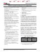
Product Folder Sample & Buy Technical Documents Support & Community Tools & Software TPS659110, TPS659112, TPS659113, TPS659116 SWCS049L – JUNE 2010 – REVISED MARCH 2014 TPS65911x Integrated Power Management Unit Top Specification 1 Features The purpose of the TPS65911 device is to provide the following resources: • 1 • • • • • • • • • • • • • • Embedded power controller (EPC) with EEPROM programmability Two efficient step-down DCDC converters for processor cores (VDD1, VDD2) One efficient ste
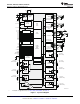
TPS659110, TPS659112, TPS659113, TPS659116 www.ti.com VBACKUP SWCS049L – JUNE 2010 – REVISED MARCH 2014 CBB VCC7 VCC1 1.5 A @ 0.6 to 2.2 V* VRTC VRTC (LDO) and POR BACKUP Mgmt AGND VDD1 3 SW1 GND1 AGND 0.6 to 1.5 V, 12.5-mV step VFB1 1.5 A @ 0.6 to 1.5 V* VCC2 OSC32KIN OSC 32-kHz OSC32KOUT REFGND Real time clock VDDIO SDA_SDI 3 SW2 GND2 0.6 to 1.5 V, 12.5-mV step, 1.
TPS659110, TPS659112, TPS659113, TPS659116 www.ti.com SWCS049L – JUNE 2010 – REVISED MARCH 2014 Table of Contents 1 2 3 4 5 Features ................................................................. Applications .......................................................... Description ............................................................ Revision History ................................................... Terminal Configuration and Functions ............... 5.1 5.2 5.3 5.4 5.5 5.6 5.7 5.8 5.9 5.10 5.
TPS659110, TPS659112, TPS659113, TPS659116 SWCS049L – JUNE 2010 – REVISED MARCH 2014 www.ti.com Table 2.
TPS659110, TPS659112, TPS659113, TPS659116 www.ti.
TPS659110, TPS659112, TPS659113, TPS659116 SWCS049L – JUNE 2010 – REVISED MARCH 2014 www.ti.
TPS659110, TPS659112, TPS659113, TPS659116 www.ti.com SWCS049L – JUNE 2010 – REVISED MARCH 2014 Table 3.
TPS659110, TPS659112, TPS659113, TPS659116 SWCS049L – JUNE 2010 – REVISED MARCH 2014 www.ti.com Table 3.
TPS659110, TPS659112, TPS659113, TPS659116 www.ti.com SWCS049L – JUNE 2010 – REVISED MARCH 2014 Table 3.
TPS659110, TPS659112, TPS659113, TPS659116 SWCS049L – JUNE 2010 – REVISED MARCH 2014 www.ti.com 5.1 Absolute Maximum Ratings Stresses beyond those listed under below may cause permanent damage to the device. These are stress ratings only and functional operation of the device at these or any other conditions beyond those indicated below are not implied. Exposure to absolute-maximum-rated conditions for extended periods may affect device reliability.
TPS659110, TPS659112, TPS659113, TPS659116 www.ti.com SWCS049L – JUNE 2010 – REVISED MARCH 2014 5.2 Recommended Operating Conditions Lists of the recommended operating maximum ratings, over operating free-air temperature range (unless otherwise noted), for the TPS65911 device are given below. Note: VCC7 should be connected to highest supply that is connected to device VCCx pin. Exception: VCC4, VCC5, and V5IN inputs can be higher than VCC7.
TPS659110, TPS659112, TPS659113, TPS659116 SWCS049L – JUNE 2010 – REVISED MARCH 2014 www.ti.com External Component Recommendation (continued) For crystal oscillator components, see 32-kHz RTC Clock. Note: VCC7 supply should have enough capacitance to quarantee that when supply is switched off, voltage will not fall at a rate faster than 10 mV/ms.
TPS659110, TPS659112, TPS659113, TPS659116 www.ti.com SWCS049L – JUNE 2010 – REVISED MARCH 2014 External Component Recommendation (continued) For crystal oscillator components, see 32-kHz RTC Clock. Note: VCC7 supply should have enough capacitance to quarantee that when supply is switched off, voltage will not fall at a rate faster than 10 mV/ms.
TPS659110, TPS659112, TPS659113, TPS659116 SWCS049L – JUNE 2010 – REVISED MARCH 2014 www.ti.com 5.5 I/O Pullup And Pulldown Characteristics over operating free-air temperature range (unless otherwise noted) PARAMETER (1) TEST CONDITIONS SDA_SDI, SCL_SCK, SDASR_EN2, SCLSR_EN1 external pullup resistor Connected to VDDIO SDA_SDI, SCL_SCK, SDASR_EN2, SCLSR_EN1 Programmable pullup (DFT, default inactive) Grounded, VDDIO = 1.8 V SLEEP, PWRHOLD, programmable pulldown (default active) MIN TYP MAX 1.
TPS659110, TPS659112, TPS659113, TPS659116 www.ti.com SWCS049L – JUNE 2010 – REVISED MARCH 2014 5.6 Digital I/O Voltage Electrical Characteristics over operating free-air temperature range (unless otherwise noted) PARAMETER MIN TYP MAX UNIT 0.3 x VBAT V Related I/Os: PWRON Low-level input voltage VIL High-level input voltage VIH 0.7 x VBAT V Related I/Os: PWRHOLD, GPIO0-8, PWRDN Low-level input voltage VIL 0.
TPS659110, TPS659112, TPS659113, TPS659116 SWCS049L – JUNE 2010 – REVISED MARCH 2014 www.ti.com 5.7 I2C Interface And Control Signals over operating free-air temperature range (unless otherwise noted) NO. TEST CONDITIONS (1) (2) PARAMETER MIN TYP MAX INT1 rise and fall times, CL = 5 to 35 pF 5 10 ns NRESPWRON rise and fall times, CL = 5 to 35 pF 5 10 ns 10 80 ns 3.
TPS659110, TPS659112, TPS659113, TPS659116 www.ti.com SWCS049L – JUNE 2010 – REVISED MARCH 2014 5.8 Power Consumption over operating free-air temperature range (unless otherwise noted) All current consumption measurements are relative to the FULL chip, all VCC inputs set to VBAT voltage, COMP2 is off. PARAMETER Device BACKUP state Device OFF state Device SLEEP state TEST CONDITIONS MIN TYP MAX UNIT VBAT = 2.4 V, VBACKUP = 0 V, 13 18 µA VBAT = 0 V, VBACKUP = 3.2 V, V5IN = 0 V 7 10 VBAT = 3.
TPS659110, TPS659112, TPS659113, TPS659116 SWCS049L – JUNE 2010 – REVISED MARCH 2014 www.ti.com Power References And Thresholds (continued) over operating free-air temperature range (unless otherwise noted) PARAMETER TEST CONDITIONS Main battery discharged threshold VMBDCH2 (programmable) MIN TYP MAX UNIT Measured on VCC7 terminal (MTL prg) Triggering monitored through INT1 VMBDCH2_SEL=11000 to 11111 3.5 VMBDCH2_SEL=10111 3.45 ... VMBDCH2_SEL=01110 ... –2% 3 ... V +2% ...
TPS659110, TPS659112, TPS659113, TPS659116 www.ti.com SWCS049L – JUNE 2010 – REVISED MARCH 2014 5.
TPS659110, TPS659112, TPS659113, TPS659116 SWCS049L – JUNE 2010 – REVISED MARCH 2014 www.ti.com 5.12 Backup Battery Charger over operating free-air temperature range (unless otherwise noted) PARAMETER TEST CONDITIONS MIN TYP MAX UNIT Backup battery charging current VBACKUP = 0 to 2.8 V, BBCHEN = 1 350 650 900 µA End-of-charge backup battery voltage VCC5 = 3.6 V, IVBACKUP = –10 µA, BBSEL = 10 –3% 3.15 +3% VCC5 = 3.6 V, IVBACKUP = –10 µA, BBSEL = 00 –3% 3 +3% VCC5 = 3.
TPS659110, TPS659112, TPS659113, TPS659116 www.ti.com SWCS049L – JUNE 2010 – REVISED MARCH 2014 5.14 VIO SMPS over operating free-air temperature range (unless otherwise noted) PARAMETER TEST CONDITIONS Input voltage (VCCIO and VCC7) VIN VOUT = 1.5 V, 1.8 V, or 2.5 V VOUT = 3.3 V MIN TYP MAX 2.7 5.5 VOUT 5.5 UNIT V PWM mode (VIO_PSKIP = 0) or pulse skip mode IOUT = 0 to IMAX DC output voltage (VOUT) VSEL= 00 –3% 1.5 +3% VSEL = 01 –3% 1.8 +3% VSEL = 10 –3% 2.
TPS659110, TPS659112, TPS659113, TPS659116 SWCS049L – JUNE 2010 – REVISED MARCH 2014 www.ti.com VIO SMPS (continued) over operating free-air temperature range (unless otherwise noted) PARAMETER Ground current (IQ) TEST CONDITIONS MIN TYP Off MAX UNIT 1 PWM mode, IOUT = 0 mA, VIN = 3.8 V, VIO_PSKIP = 0 7500 PFM (Pulse Skipping) mode, no switching, 3MHz clock on 250 µA Low-power (pulse skipping) mode, no switching ST[1:0]=11 Conversion efficiency 63 PWM mode, DCRL < 50 mΩ, VOUT = 1.
TPS659110, TPS659112, TPS659113, TPS659116 www.ti.com SWCS049L – JUNE 2010 – REVISED MARCH 2014 5.15 VDD1 SMPS over operating free-air temperature range (unless otherwise noted) PARAMETER TEST CONDITIONS Input voltage (VCC1 and VCC7) VIN DC output voltage (VOUT) MIN TYP MAX VOUT ≤ 2.7 V 2.7 5.5 VOUT > 2.7 V VOUT 5.5 UNIT V VGAIN_SEL = 00, IOUT = 0 to IOUTmax: max programmable voltage, SEL[6:0] = 1001011 1.5 –3% 1.2 min programmable voltage, SEL[6:0] = 0000011 +3% V 0.
TPS659110, TPS659112, TPS659113, TPS659116 SWCS049L – JUNE 2010 – REVISED MARCH 2014 www.ti.com VDD1 SMPS (continued) over operating free-air temperature range (unless otherwise noted) PARAMETER TEST CONDITIONS DC line regulation Transient load regulation MIN TYP MAX On mode, VIN = VINmin to VINmax @ IOUT = 1500 mA VDD1 output voltage = {0.6 to 1.5 V} 20 On mode, VIN = VINmin to VINmax @ IOUT = 2000 mA VDD1 output voltage = {1.2V, 1.35 V, 1.
TPS659110, TPS659112, TPS659113, TPS659116 www.ti.com SWCS049L – JUNE 2010 – REVISED MARCH 2014 5.16 VDD2 SMPS over operating free-air temperature range (unless otherwise noted) PARAMETER TEST CONDITIONS Input voltage (VCC2 and VCC7) VIN VOUT ≤ 2.7 V VOUT > 2.7 V DC output voltage (VOUT) MIN TYP 2.7 5.5 VOUT 5.5 –3% 1.2 +3% 0.6 SEL[6:0] = 000000: power down V 0 VGAIN_SEL = 10, SEL = 0101011 = 43 –3% 2.2 +3% VGAIN_SEL = 11, SEL=0101011=43 –3% 3.
TPS659110, TPS659112, TPS659113, TPS659116 SWCS049L – JUNE 2010 – REVISED MARCH 2014 www.ti.com VDD2 SMPS (continued) over operating free-air temperature range (unless otherwise noted) PARAMETER TEST CONDITIONS MIN TYP Duty cycle UNIT 100% Minimum On time 35 P-Channel MOSFET Discharge resistor for power-down sequence RDIS 30 VFB2 internal resistance Ground current (IQ) MAX 0.5 50 1 Off PWM mode, IOUT = 0 mA, VIN = 3.
TPS659110, TPS659112, TPS659113, TPS659116 www.ti.com SWCS049L – JUNE 2010 – REVISED MARCH 2014 5.17 VDDCtrl SMPS over operating free-air temperature range (unless otherwise noted) PARAMETER TEST CONDITIONS Input Voltage for external FETs VIN Input voltage V5IN DC output voltage (VOUT) MIN TYP MAX UNIT 3 25 V 4.5 5.5 V IOUT = 0 to IOUTmax: max programmable voltage: SEL[6:0]=1000011 to 1111111 1.4 ... SEL[6:0]=0110001 1.2 V ... min programmable voltage: SEL[6:0]=0000001 to 0000011 0.
TPS659110, TPS659112, TPS659113, TPS659116 SWCS049L – JUNE 2010 – REVISED MARCH 2014 www.ti.com VDDCtrl SMPS (continued) over operating free-air temperature range (unless otherwise noted) PARAMETER TEST CONDITIONS MIN TYP MAX UNIT OUTPUT DRIVERS R(DRVH) DRVH resistance R(DRVL) DRVL resistance tD Dead time Source, I(DRVH) = –50 mA 1.5 3 Sink, I(DRVH) = 50 mA 0.7 1.8 1 2.2 Source, I(DRVL) = –50 mA Sink, I(DRVL) = 50 mA 0.5 1.
TPS659110, TPS659112, TPS659113, TPS659116 www.ti.com SWCS049L – JUNE 2010 – REVISED MARCH 2014 5.18 LDO1 And LDO2 over operating free-air temperature range (unless otherwise noted) PARAMETER Input voltage (VCC6) VIN TEST CONDITIONS MIN VOUT(LDO1) = 1.05 V @ 320 mA and VOUT(LDO2) = 1.05 V @ 160 mA 1.4 3.6 VOUT(LDO1) = 1.2 V/1.5 V @ 100 mA and VOUT(LDO2) = 1.2 V/1.1 V/1.0 V 1.7 3.6 VOUT(LDO1) = 1.5 V and VOUT (LDO1, LDO2) = 1.8 V @ 200 mA 2.1 3.6 VOUT(LDO1) = 1.8 V and VOUT(LDO2) = 1.8 V 2.
TPS659110, TPS659112, TPS659113, TPS659116 SWCS049L – JUNE 2010 – REVISED MARCH 2014 www.ti.com LDO1 And LDO2 (continued) over operating free-air temperature range (unless otherwise noted) PARAMETER TEST CONDITIONS MIN (VINmax = 3.6 V) TYP MAX UNIT 1.05 –3% ... +3% 3.25 3.
TPS659110, TPS659112, TPS659113, TPS659116 www.ti.com SWCS049L – JUNE 2010 – REVISED MARCH 2014 5.19 LDO3 And LDO4 over operating free-air temperature range (unless otherwise noted) PARAMETER Input voltage (VCC5) VIN TEST CONDITIONS MIN TYP MAX VOUT (LDO3) = 1.8 V and VOUT (LDO4) = 1.8 V/ 1.1 V/ 1.0 V 2.7 5.5 VOUT (LDO3) = 2.6 V and VOUT (LDO4) = 2.5 V 3.0 5.5 VOUT (LDO3) = 2.8 V 3.2 5.5 UNIT V LDO3 DC output voltage VOUT On and low-power mode, VOUT = 1.0 – 3.
TPS659110, TPS659112, TPS659113, TPS659116 SWCS049L – JUNE 2010 – REVISED MARCH 2014 www.ti.com LDO3 And LDO4 (continued) over operating free-air temperature range (unless otherwise noted) PARAMETER Rated output current IOUTmax TEST CONDITIONS MIN On mode 50 Low-power mode 1 Load current limitation (shortcircuit protection) On mode, VOUT = VOUTmin – 100 mV Dropout voltage VDO On mode, VOUTtyp = 2.5 V, VDO = VIN – VOUT 200 TYP MAX mA 400 500 100 160 VIN = 3.
TPS659110, TPS659112, TPS659113, TPS659116 www.ti.com SWCS049L – JUNE 2010 – REVISED MARCH 2014 5.20 LDO5 over operating free-air temperature range (unless otherwise noted) PARAMETER Input voltage (VCC4) VIN TEST CONDITIONS MIN TYP MAX VOUT (LDO5) = 1.8 V 2.7 5.5 VOUT (LDO5) = 2.5 V 3.2 5.5 VOUT (LDO5) = 2.8 V @ Iload = 200 mA 3.2 5.5 VOUT (VAUX2) = 2.8 V @ 300 mA 3.2 5.5 UNIT V LDO5 DC output voltage VOUT On and low-power mode, VOUT = 1.0 – 3.3 V, VIN = VINmin to VINmax 1 1.1 –3% ..
TPS659110, TPS659112, TPS659113, TPS659116 SWCS049L – JUNE 2010 – REVISED MARCH 2014 www.ti.com 5.21 LDO6, LDO7, And LDO8 over operating free-air temperature range (unless otherwise noted) PARAMETER Input voltage (VCC3) VIN TEST CONDITIONS MIN VOUT(LDO6) = 1.2 V @ 150 mA, VOUT(LDO7) = 1.1 V @ 150 mA and (VLDO8) = 1 V @ 180 mA 1.7 5.5 VOUT(LDO7) = 1.8 V/2 V and VOUT(LDO6) = 1.8 V 2.7 5.5 VOUT(LDO7) = 2.8 V 3.2 5.5 VOUT(LDO7) = 3.3 V 3.6 5.5 VOUT(LDO7) = 2.8 V @ 250 mA 3.2 5.
TPS659110, TPS659112, TPS659113, TPS659116 www.ti.com SWCS049L – JUNE 2010 – REVISED MARCH 2014 LDO6, LDO7, And LDO8 (continued) over operating free-air temperature range (unless otherwise noted) PARAMETER TEST CONDITIONS MIN TYP MAX UNIT 1.1 –3% ... +3% 3.2 V 3.3 Rated output current IOUTmax On mode 300 Low-power mode mA 1 Load current limitation (shortcircuit protection) On mode, VOUT = VOUTmin – 100 mV Dropout voltage VDO On mode, VDO = VIN – VOUT, 450 550 650 VIN = 2.
TPS659110, TPS659112, TPS659113, TPS659116 SWCS049L – JUNE 2010 – REVISED MARCH 2014 www.ti.com LDO6, LDO7, And LDO8 (continued) over operating free-air temperature range (unless otherwise noted) PARAMETER Dropout voltage VDO TEST CONDITIONS MIN TYP MAX UNIT On mode, VDO = VIN – VOUT, VIN = 2.7 V, IOUT = IOUTmax 500 VIN = 2.7 V, IOUT = 250 mA 400 VIN = 2.7 V, IOUT = 200 mA 300 VIN = 1.7 V, IOUT = 180 mA 700 VIN = 1.7 V, IOUT = 150 mA 500 VIN = 1.
TPS659110, TPS659112, TPS659113, TPS659116 www.ti.com SWCS049L – JUNE 2010 – REVISED MARCH 2014 Switch-ON/-OFF Sequences And Timing (continued) tpd2 PWRHOLD tdsON1 VIO LDO5 tdsON2 VDD2 tdsON3 VDD1 tdsON4 LDO4 tdsON5 LDO3 LDO8 tdsON6 LDO6 i tdsON15 CLK32KOUT tdsON16 tpd1 NRESPWRON NRESPWRON2 tond: Switch-on sequence Switch-off sequence SWCS049-004 Note:: Figure 4 is for illustrative purposes only and does not describe any actual TPS65911x part number. Figure 4.
TPS659110, TPS659112, TPS659113, TPS659116 SWCS049L – JUNE 2010 – REVISED MARCH 2014 www.ti.com Device State Control Through PWRON Signal (continued) PWRON VIO 1.8 V CLK32KOUT NRESPWRON Interrupt acknowledge INT1 PWRON_IT=1 Interrupt acknowledge PWRON_IT=1 Internal pulse tdOINT1 PWRHOLD t dbPWRHOLDF t dbPWRONF t dSONT Switch On sequence t dONPWHOLD t dbPWRONF Switch-off sequence SWCS049-005 Note:: 1.
TPS659110, TPS659112, TPS659113, TPS659116 www.ti.com SWCS049L – JUNE 2010 – REVISED MARCH 2014 Device State Control Through PWRON Signal (continued) Table 5.
TPS659110, TPS659112, TPS659113, TPS659116 SWCS049L – JUNE 2010 – REVISED MARCH 2014 www.ti.com Device SLEEP State Control (continued) Table 6.
TPS659110, TPS659112, TPS659113, TPS659116 www.ti.com SWCS049L – JUNE 2010 – REVISED MARCH 2014 7.3 Device Turn-On/Turn-Off with Rising/Falling Input Voltage VMBCH threshold VMBDCH2 threshold VMBLO threshold VMBHI threshold VBNPR threshold VCC7 1.8 V VRTC VBACKUP > VBNPR VIO 1.
TPS659110, TPS659112, TPS659113, TPS659116 SWCS049L – JUNE 2010 – REVISED MARCH 2014 www.ti.com 7.4 Power Supplies State Control Through EN1 and EN2 Signals Switch-on sequence Switch-off sequence Device on NRESPWRON tdEN EN1 tdVEN LDO1 tdEN 1.2 V tdSOFF2 tdEN EN2 tdEN Low-power mode 1.8 V LDO4 SWCS046-009 NOTE: Register setting: LDO1_EN1 = 1, LDO4_EN2 = 1, and LDO4_KEEPON = 1. Figure 9.
TPS659110, TPS659112, TPS659113, TPS659116 www.ti.com SWCS049L – JUNE 2010 – REVISED MARCH 2014 7.5 VDD1, VDD2 Voltage Control Through EN1 and EN2 Signals EN1 tdDVSEN tdDVSENL tdDVSEN 1.2 V VDD1/VFB1 tdDVSENL 0.8 V TSTEP[2:0]=001 TSTEP[2:0]=011 SW1 PFM (pulse skipping) mode PWM mode PFM (pulse skipping) mode PWM mode PFM (pulse skipping) mode SWCS049-011 NOTE: Register setting: VDD1_EN1=1, SEL[6:0]=hex13 in VDD1_SR_REG Figure 11. VDD1 Supply Voltage Control Through EN1 Table 9.
TPS659110, TPS659112, TPS659113, TPS659116 SWCS049L – JUNE 2010 – REVISED MARCH 2014 www.ti.com 8 Detailed Description 8.1 Power Reference The bandgap voltage reference is filtered by using an external capacitor connected across the VREF output and the analog ground REFGND (see Recommended Operating Conditions). The VREF voltage is distributed and buffered inside the device. 8.
TPS659110, TPS659112, TPS659113, TPS659116 www.ti.com SWCS049L – JUNE 2010 – REVISED MARCH 2014 Embedded Power Controller (continued) • • • • reset is asserted in this case. Everything on the device is off. BACKUP: The main battery supply voltage is high enough to enable the VRTC domain but not enough to switch on all the resources. In this state, the VRTC regulator is in backup mode and only the 32K oscillator and RTC module are operating (if enabled). All other resources are off or under reset.
TPS659110, TPS659112, TPS659113, TPS659116 SWCS049L – JUNE 2010 – REVISED MARCH 2014 www.ti.com Embedded Power Controller (continued) (tDOINT1 pulse duration defined in Power Control Timing). Interrupt sources expected (if enabled), when the device is off: – RTC alarm interrupt – First-time input voltage rising above the VMBHI threshold (depending on the boot mode used) and input voltage > VMBCH threshold. The interrupt corresponding to this last condtion is VMBCH_IT in the INT_STS_REG register.
TPS659110, TPS659112, TPS659113, TPS659116 www.ti.com SWCS049L – JUNE 2010 – REVISED MARCH 2014 Embedded Power Controller (continued) Power off disables all power resources at the same time by default. By setting the PWR_OFF_SEQ control bit to 1, power off will follow the power-up sequence in reverse order (the first resource to be powered on will be last to power off). The values of VDD1, VDD2, and VDDCtrl set in the boot sequence can be selected from 16 steps.
TPS659110, TPS659112, TPS659113, TPS659116 SWCS049L – JUNE 2010 – REVISED MARCH 2014 www.ti.com Table 11. Boot Configuration: Power Sequence Control Bits (continued) Register Bit LDO4_REG SEL[7:2] EEPROM LDO5_REG SEL[6:2] 1.2 V x 2 x LDO5 voltage: 1 V x LDO4 voltage selection LDO5 voltage selection Off x LDO6 voltage: 1 V x Off x 1.2 V x 5 x 1.
TPS659110, TPS659112, TPS659113, TPS659116 www.ti.com SWCS049L – JUNE 2010 – REVISED MARCH 2014 Table 12. Boot Configuration: General Control Bits (continued) Register INT_MSK3_REG INT_MSK3_REG INT_MSK3_REG Bit GPIO5_F_IT_MSK GPIO5_R_IT_MSK GPIO4_F_IT_MSK INT_MSK3_REG GPIO4_R_IT_MSK GPIO0_REG GPIO_ODEN WATCHDOG_REG WATCHDOG_EN Description TPS65911x Fixed Boot EEPROM Boot 1 x 0 x 1 x 0 x Push-pull x 1 x Disable buffer x 3.
TPS659110, TPS659112, TPS659113, TPS659116 SWCS049L – JUNE 2010 – REVISED MARCH 2014 www.ti.com 8.3.3.2 PWRHOLD The PWRHOLD pin can be used as a PWRHOLD signal input or as a general purpose input (GPI). The mode is selected by the AUTODEV_ON bit, which is part of the boot configuration. When AUTODEV_MODE = 0, the PWRHOLD feature is selected.
TPS659110, TPS659112, TPS659113, TPS659116 www.ti.com SWCS049L – JUNE 2010 – REVISED MARCH 2014 For a description of interrupt sources, see Table 14. 8.3.3.8 EN2 and EN1 EN2 and EN1 are the data and clock signals of the serial control interface dedicated to voltage scaling applications. These signals can also be programmed to be used as enable signals of one or several supplies, when the device is on (NRESPWRON high).
TPS659110, TPS659112, TPS659113, TPS659116 SWCS049L – JUNE 2010 – REVISED MARCH 2014 www.ti.com 8.3.3.12 Comparators: COMP1 and COMP2 The TPS65911 device has three comparators for system status detection/control. One comparator detects the voltage at pin VCC7. When VCC7 > VMBHI, the comparator initiates a NO SUPPLY-to-OFF transition and the VMBHI_IT interrupt is generated. When VCC7 < VMBLO, the comparator initiates an ACTIVE/SLEEP/OFF-toBACKUP transition.
TPS659110, TPS659112, TPS659113, TPS659116 www.ti.com SWCS049L – JUNE 2010 – REVISED MARCH 2014 Periodic mode: WTCHDG_CNT 0 1 N 0 1 N 1 N WTCHDG_IT WTCHDG_OFF WTCHDG_IT clearing interrupt clearing Interrupt mode: WTCHDG_CNT 0 1 i 0 WTCHDG_OFF SWCS049-013 Figure 13. Watchdog Signals 8.3.3.14 Tracking LDO LDO4 has an optional mode where its output level follows that of VDD1, from 0.6 to 1.5 V, when VDD1 is active.
TPS659110, TPS659112, TPS659113, TPS659116 SWCS049L – JUNE 2010 – REVISED MARCH 2014 www.ti.com 8.5 Dynamic Voltage Frequency Scaling And Adaptive Voltage Scaling Operation Dynamic voltage frequency scaling (DVFS) operation: A supply voltage value corresponding to a targeted frequency of the digital core supplied is programmed in VDD1_OP_REG or VDD2_OP_REG registers. The slew rate of the voltage supply reaching a new VDD1_OP_REG or VDD2_OP_REG programmed value is limited to 12.5 mV/µs, fixed value.
TPS659110, TPS659112, TPS659113, TPS659116 www.ti.com SWCS049L – JUNE 2010 – REVISED MARCH 2014 32-kHz RTC Clock (continued) VRTC 32 kHz to digital block Biasing and amplitude control OSC32KIN REFGND OSC32KOUT Q COSCIN COSCOUT SWCS049-014 Figure 15. Crystal Oscillator 32-kHz Clock 8.7 Real-Time Clock (RTC) The RTC, which is driven by the 32-kHz clock, provides the alarm and timekeeping functions. The RTC is kept supplied when the device is in the OFF or the BACKUP state.
TPS659110, TPS659112, TPS659113, TPS659116 SWCS049L – JUNE 2010 – REVISED MARCH 2014 www.ti.com Real-Time Clock (RTC) (continued) 32-kHz clock input Frequency compensation 32-kHz counter Seconds Minutes Hours Interrupt Week Days Control Days Months Alarm Years INT_ALARM INT_TIMER SWCS049-015 Figure 16. RTC Digital Section Block Diagram 8.7.1 Time Calendar Registers All the time and calendar information is available in these dedicated registers, called TC registers.
TPS659110, TPS659112, TPS659113, TPS659116 www.ti.com SWCS049L – JUNE 2010 – REVISED MARCH 2014 Table 13. Real-Time Clock Registers Example (continued) Register Value MONTHS_REG 0x09 YEARS_REG 0x08 The user can round to the closest minute, by setting the ROUND_30S register bit. TC values are set to the closest minute value at the next second. The ROUND_30S bit is automatically cleared when the rounding time is performed.
TPS659110, TPS659112, TPS659113, TPS659116 SWCS049L – JUNE 2010 – REVISED MARCH 2014 www.ti.com NOTE The compensation is considered once written into the registers. 8.8 Backup Battery Management The device includes a back-up battery switch connecting the VRTC regulator input to a main battery (VCC7) or to a back-up battery (VBACKUP), depending on the voltage value of the battery. The VRTC supply can then be maintained during a BACKUP state as long as the input voltage is high enough (> VBNPR threshold).
TPS659110, TPS659112, TPS659113, TPS659116 www.ti.
TPS659110, TPS659112, TPS659113, TPS659116 SWCS049L – JUNE 2010 – REVISED MARCH 2014 www.ti.
TPS659110, TPS659112, TPS659113, TPS659116 www.ti.com SWCS049L – JUNE 2010 – REVISED MARCH 2014 Interrupts (continued) Table 14. Interrupt Sources (continued) Interrupt Description VMBDCH_IT The battery voltage fall down below the VMBDCH threshold: the minimum operating voltage of power supplies.
TPS659110, TPS659112, TPS659113, TPS659116 SWCS049L – JUNE 2010 – REVISED MARCH 2014 www.ti.com 9 Package Description The following are the package descriptions of the TPS65911 PMU devices: • Package type: Package TPS65911 Type ZRC98 BGA Microstar Junior Size (mm) 6x9 Substrate layers 1 layer Pitch ball array (mm) 0.65 mm Number of balls 98 Thickness (mm) (max. height including balls) 1 9.
TPS659110, TPS659112, TPS659113, TPS659116 www.ti.com SWCS049L – JUNE 2010 – REVISED MARCH 2014 10 PCB Layout The package ballout of the TPS65911 supports the use of inexpensive 4-layer, non-HID board technology. Figure 22 shows an example layout. Regardless of the chosen board technology, special care must be taken when designing the board layout for the TPS65911 to ensure performance. For detailed guidelines, see TPS65911 Layout Guidelines, TI Literature number SWCU080. Figure 22.
TPS659110, TPS659112, TPS659113, TPS659116 SWCS049L – JUNE 2010 – REVISED MARCH 2014 www.ti.com 11 Appendix A: Functional Registers The possible device reset domains are: • Full reset: All digital logic of device is reset. – Caused by POR (power on reset) when VCC7 < VBNPR and BB < VBNPR • General reset: No impact on RTC, backup registers or interrupt status.
TPS659110, TPS659112, TPS659113, TPS659116 www.ti.com SWCS049L – JUNE 2010 – REVISED MARCH 2014 11.1 TPS65911_FUNC_REG Registers Mapping Summary Table 15.
TPS659110, TPS659112, TPS659113, TPS659116 SWCS049L – JUNE 2010 – REVISED MARCH 2014 www.ti.com TPS65911_FUNC_REG Registers Mapping Summary (continued) Table 15.
TPS659110, TPS659112, TPS659113, TPS659116 www.ti.com SWCS049L – JUNE 2010 – REVISED MARCH 2014 Table 16.
TPS659110, TPS659112, TPS659113, TPS659116 SWCS049L – JUNE 2010 – REVISED MARCH 2014 www.ti.com Table 19.
TPS659110, TPS659112, TPS659113, TPS659116 www.ti.com SWCS049L – JUNE 2010 – REVISED MARCH 2014 7 6 5 4 3 2 1 Reserved 0 WEEK Bits Field Name Description Type Reset 7:3 Reserved Reserved bit RO R returns 0s 0x00 2:0 WEEK First digit of day of the week (range is 0 up to 6) RW 0 Table 23.
TPS659110, TPS659112, TPS659113, TPS659116 7 6 ALARM_PM_NAM SWCS049L – JUNE 2010 – REVISED MARCH 2014 Reserved Bits www.ti.
TPS659110, TPS659112, TPS659113, TPS659116 www.ti.com SWCS049L – JUNE 2010 – REVISED MARCH 2014 Bits Field Name Description Type Reset 7:5 Reserved Reserved bit RO R returns 0s 0x0 4 ALARM_MONTH1 Second digit of alarm programmation for months (range is 0 up to 1) RW 0 3:0 ALARM_MONTH0 First digit of alarm programmation for months (range is 0 up to 9) RW 0x1 Table 28.
TPS659110, TPS659112, TPS659113, TPS659116 SWCS049L – JUNE 2010 – REVISED MARCH 2014 Bits www.ti.com Field Name Description Type Reset 3 MODE_12_24 0: 24 hours mode 1: 12 hours mode (PM-AM mode) It is possible to switch between the two modes at any time without disturbed the RTC, read or write are always performed with the current mode.
TPS659110, TPS659112, TPS659113, TPS659116 SWCS049L – JUNE 2010 – REVISED MARCH 2014 7 6 5 Reserved 4 3 2 IT_SLEEP_MASK_EN www.ti.com 1 IT_ALARM IT_TIMER 0 EVERY Bits Field Name Description Type Reset 7:5 Reserved Reserved bit RO R returns 0s 0x0 4 IT_SLEEP_MASK_E N 1: Mask periodic interrupt while the TPS65911 device is in SLEEP mode. Interrupt event is back up in a register and occurred as soon as the TPS65911 device is no more in SLEEP mode.
TPS659110, TPS659112, TPS659113, TPS659116 SWCS049L – JUNE 2010 – REVISED MARCH 2014 7 6 www.ti.com 5 4 3 2 1 0 RTC_COMP_MSB Bits Field Name Description 7:0 RTC_COMP_MSB This register contains the number of 32-kHz periods to be added into the 32-kHz counter every hour [MSB] Type Reset RW 0x00 Table 34.
TPS659110, TPS659112, TPS659113, TPS659116 www.ti.com SWCS049L – JUNE 2010 – REVISED MARCH 2014 7 6 5 4 3 2 1 0 BCKUP Bits Field Name Description 7:0 BCKUP Backup bit Type Reset RW 0x00 Table 37. BCK2_REG Address Offset 0x18 Physical Address Instance (RESET DOMAIN: FULL RESET) Description Backup register which can be used for storage by the application firmware when the external host is powered down. These registers will retain their content as long as the VRTC is active.
TPS659110, TPS659112, TPS659113, TPS659116 SWCS049L – JUNE 2010 – REVISED MARCH 2014 7 6 www.ti.com 5 4 3 2 1 0 BCKUP Bits Field Name Description 7:0 BCKUP Backup bit Type Reset RW 0x00 Table 41. PUADEN_REG 0x1C Physical Address Instance Description Pullup/pulldown control register.
TPS659110, TPS659112, TPS659113, TPS659116 www.ti.com SWCS049L – JUNE 2010 – REVISED MARCH 2014 Bits Field Name Description Type Reset 7:2 Reserved Reserved bit RO R returns 0s 0x00 1:0 ST Reference state: ST[1:0] = 00: Off ST[1:0] = 01: On high power (ACTIVE) ST[1:0] = 10: Reserved ST[1:0] = 11: On low power (SLEEP) (Write access available in test mode only) RO 0x1 Table 43.
TPS659110, TPS659112, TPS659113, TPS659116 SWCS049L – JUNE 2010 – REVISED MARCH 2014 www.ti.com Bits Field Name Description 7:6 ILMAX Select maximum load current: when 00: 0.6 A when 01: 1.0 A when 10: 1.3 A when 11: 1.3 A Type Reset RW 0x0 5:4 Reserved Reserved bit RO R returns 0s 0x0 3:2 SEL Output voltage selection (EEPROM bits): SEL[1:0] = 00: 1.5 V SEL[1:0] = 01: 1.8 V SEL[1:0] = 10: 2.5 V SEL[1:0] = 11: 3.
TPS659110, TPS659112, TPS659113, TPS659116 www.ti.com SWCS049L – JUNE 2010 – REVISED MARCH 2014 Table 46. VDD1_OP_REG (continued) Description VDD1 voltage selection register. This register can be accessed by both control and coltage scaling I2C interfaces depending on SR_CTL_I2C_SEL register bit value.
TPS659110, TPS659112, TPS659113, TPS659116 SWCS049L – JUNE 2010 – REVISED MARCH 2014 www.ti.com Table 48.
TPS659110, TPS659112, TPS659113, TPS659116 www.ti.com Bits SWCS049L – JUNE 2010 – REVISED MARCH 2014 Field Name Description Type Reset 7 CMD Command: when 0: VDD2_OP_REG voltage is applied when 1: VDD2_SR_REG voltage is applied RW 0 6:0 SEL Output voltage (4 EEPROM bits) selection with GAIN_SEL = 00 (G = 1, 12.5 mV per LSB): SEL[6:0] = 1001011 to 1111111: 1.5 V ... SEL[6:0] = 0111111: 1.35 V ... SEL[6:0] = 0110011: 1.2 V ... SEL[6:0] = 0000001 to 0000011: 0.6 V SEL[6:0] = 0000000: Off (0.
TPS659110, TPS659112, TPS659113, TPS659116 SWCS049L – JUNE 2010 – REVISED MARCH 2014 www.ti.com Bits Field Name Description Type Reset 7:2 Reserved Reserved bit RO R returns 0s 0x00 1:0 ST Supply state (EEPROM dependent): ST[1:0] = 00: Off ST[1:0] = 01: On ST[1:0] = 10: Off ST[1:0] = 11: On RW 0x0 Table 52. VDDCRTL_OP_REG Address Offset 0x28 Physical Address Instance (RESET DOMAIN: TURN OFF RESET) Description VDDCtrl voltage selection register.
TPS659110, TPS659112, TPS659113, TPS659116 www.ti.com Bits SWCS049L – JUNE 2010 – REVISED MARCH 2014 Field Name 7 Description Reserved 6:0 SEL Output voltage (4 EEPROM bits) selection: SEL[6:0] = 1000011 to 1111111: 1.4 V ... SEL[6:0] = 0110011: 1.2 V ... SEL[6:0] = 0010011: 0.8 V ... SEL[6:0] = 0000001: 0000011: 0.6 V SEL[6:0] = 0000000: Off (0.0 V) Note: from SEL[6:0] = 3 to 64 (dec) Vout= (SEL[6:0] × 12.5 mV + 0.
TPS659110, TPS659112, TPS659113, TPS659116 SWCS049L – JUNE 2010 – REVISED MARCH 2014 www.ti.com Bits Field Name Description 1:0 ST Supply state (EEPROM bits): ST[1:0] = 00: Off ST[1:0] = 01: On high power (ACTIVE) ST[1:0] = 10: Off ST[1:0] = 11: On low power (SLEEP) Type Reset RW 0x0 Table 56.
TPS659110, TPS659112, TPS659113, TPS659116 www.ti.com SWCS049L – JUNE 2010 – REVISED MARCH 2014 Bits Field Name Description 1:0 ST Supply state (EEPROM bits): ST[1:0] = 00: Off ST[1:0] = 01: On high power (ACTIVE) ST[1:0] = 10: Off ST[1:0] = 11: On low power (SLEEP) Type Reset RW 0x0 Table 58.
TPS659110, TPS659112, TPS659113, TPS659116 SWCS049L – JUNE 2010 – REVISED MARCH 2014 www.ti.com Bits Field Name Description 1:0 ST Supply state (EEPROM bits): ST[1:0] = 00: Off ST[1:0] = 01: On high power (ACTIVE) ST[1:0] = 10: Off ST[1:0] = 11: On low power (SLEEP) Type Reset RW 0x0 Table 60.
TPS659110, TPS659112, TPS659113, TPS659116 www.ti.com SWCS049L – JUNE 2010 – REVISED MARCH 2014 Bits Field Name Description 1:0 ST Supply state (EEPROM bits): ST[1:0] = 00: Off ST[1:0] = 01: On high power (ACTIVE) ST[1:0] = 10: Off ST[1:0] = 11: On low power (SLEEP) Type Reset RW 0x0 Table 62.
TPS659110, TPS659112, TPS659113, TPS659116 SWCS049L – JUNE 2010 – REVISED MARCH 2014 www.ti.com Bits Field Name Description Type Reset 7:3 Reserved Reserved bit RO R returns 0s 0x00 2:1 BBSEL Back up battery charge voltage selection: BBSEL[1:0] = 00: 3.0 V BBSEL[1:0] = 01: 2.52 V BBSEL[1:0] = 10: 3.15 V BBSEL[1:0] = 11: VBAT RW 0x0 BBCHEN Back up battery charge enable RW 0 0 Table 64.
TPS659110, TPS659112, TPS659113, TPS659116 7 6 5 4 3 2 1 0 RTC_PWDN CK32K_CTRL SR_CTL_I2C_SEL DEV_OFF_RST SWCS049L – JUNE 2010 – REVISED MARCH 2014 PWR_OFF_SEQ www.ti.com DEV_ON DEV_SLP DEV_OFF Bits Field Name Description Type Reset 7 PWR_OFF_SEQ When 1, power-off will be sequencial, reverse of power-on sequence (first resource to power on will be the last to power off).
TPS659110, TPS659112, TPS659113, TPS659116 SWCS049L – JUNE 2010 – REVISED MARCH 2014 Bits Field Name www.ti.com Description Type Reset RO R returns 0s 0 When 1, DCDC output level in SLEEP mode is VDDx_SR_REG, to be other than 0 V.
TPS659110, TPS659112, TPS659113, TPS659116 www.ti.
TPS659110, TPS659112, TPS659113, TPS659116 SWCS049L – JUNE 2010 – REVISED MARCH 2014 www.ti.com Table 69. SLEEP_SET_LDO_OFF_REG Address Offset 0x43 Physical Address Instance (RESET DOMAIN: GENERAL RESET) Description Configuration Register turning-off LDO regulator during the SLEEP state of the device.
TPS659110, TPS659112, TPS659113, TPS659116 www.ti.com Bits 7 6:5 SWCS049L – JUNE 2010 – REVISED MARCH 2014 Field Name Description DEFAULT_VOLT When 1, default voltages (register value after switch-on) will be applied to all resources during SLEEP-to-ACTIVE transition. When 0, voltages programmed before the ACTIVE-to-SLEEP state transition will be used to turned-on supplies during SLEEP-to-ACTIVE state transition.
TPS659110, TPS659112, TPS659113, TPS659116 SWCS049L – JUNE 2010 – REVISED MARCH 2014 www.ti.com Table 72. EN1_SMPS_ASS_REG (continued) Configuration Register setting the SMPS Supplies driven by the multiplexed SCLSR_EN1 signal. When control bit = 1, SMPS Supply state and voltage is driven by the SCLSR_EN1 control signal and is also defined though SLEEP_KEEP_RES_ON register setting. When control bit = 0 no effect: SMPS Supply state is driven though registers programming and the device state.
TPS659110, TPS659112, TPS659113, TPS659116 www.ti.com SWCS049L – JUNE 2010 – REVISED MARCH 2014 Table 73. EN2_LDO_ASS_REG (continued) Description Configuration Register setting the LDO regulators, driven by the multiplexed SDASR_EN2 signal.
TPS659110, TPS659112, TPS659113, TPS659116 SWCS049L – JUNE 2010 – REVISED MARCH 2014 Bits www.ti.com Field Name Description Type Reset 3 VDDCTRL_EN2 When control bit = 1: When EN2 is high the supply voltage is programmed though VDDCtrl_OP_REG register, and it can also be programmed off.. When EN2 is low the supply voltage is programmed though VDDCtrl_SR_REG register, and it can also be programmed off.
TPS659110, TPS659112, TPS659113, TPS659116 www.ti.com Bits SWCS049L – JUNE 2010 – REVISED MARCH 2014 Field Name Description Type Reset 4 PWRHOLD_R_IT Rising PWRHOLD event interrupt status. RW W1 to Clr 0 3 PWRON_LP_IT PWRON Long Press event interrupt status. RW W1 to Clr 0 2 PWRON_IT PWRON event interrupt status. RW W1 to Clr 0 1 VMBHI_IT VBAT > VMHI event interrupt status RW W1 to Clr 0 0 PWRHOLD_F_IT Falling PWRHOLD event interrupt status. RW W1 to Clr 0 Table 76.
TPS659110, TPS659112, TPS659113, TPS659116 SWCS049L – JUNE 2010 – REVISED MARCH 2014 www.ti.com Table 77. INT_STS2_REG Address Offset 0x52 Physical Address Instance (RESET DOMAIN: FULL RESET) Description Interrupt status register: The interrupt status bit is set to 1 when the associated interrupt event is detected. Interrupt status bit is cleared by writing 1.
TPS659110, TPS659112, TPS659113, TPS659116 www.ti.com Bits SWCS049L – JUNE 2010 – REVISED MARCH 2014 Field Name Description Type Reset 1 GPIO0_F_IT_MSK GPIO0 falling-edge detection interrupt mask. RW 1 0 GPIO0_R_IT _MSK GPIO0 rising-edge detection interrupt mask. RW 1 Table 79. INT_STS3_REG Address Offset 0x54 Physical Address Instance (RESET DOMAIN: FULL RESET) Description Interrupt status register: The interrupt status bit is set to 1 when the associated interrupt event is detected.
TPS659110, TPS659112, TPS659113, TPS659116 SWCS049L – JUNE 2010 – REVISED MARCH 2014 Bits www.ti.com Field Name Description Type Reset 7 PWRDN_IT_MSK PWRDN interrupt mask RW 1 6 VMBCH2_L_IT_MSK Comparator2 input below threshold detection interrupt mask RW 1 5 VMBCH2_H_IT_MSK Comparator2 input above threshold detection interrupt mask RW 1 4 WTCHDG_IT_MSK Watchdog interrupt mask. RW 1 3 GPIO5_F_IT_MSK GPIO5 falling-edge detection interrupt mask.
TPS659110, TPS659112, TPS659113, TPS659116 www.ti.com SWCS049L – JUNE 2010 – REVISED MARCH 2014 7 6 Reserved Bits Field Name 7:6 Reserved 5 4 3 2 1 0 GPIO_SEL GPIO_DEB GPIO_PDEN GPIO_CFG GPIO_STS GPIO_SET Description Type Reset RO R returns 0s 0x0 5 GPIO_SEL Select signal to be available at GPIO when configured as output: 0: GPIO_SET 1: LED1 out RW 0 4 GPIO_DEB GPIO input debouncing time configuration: When 0, the debouncing is 91.5 µs using a 30.
TPS659110, TPS659112, TPS659113, TPS659116 SWCS049L – JUNE 2010 – REVISED MARCH 2014 www.ti.com Table 84.
TPS659110, TPS659112, TPS659113, TPS659116 www.ti.com SWCS049L – JUNE 2010 – REVISED MARCH 2014 Table 86. GPIO5_REG Address Offset 0x65 Physical Address Instance Description GPIO5 configuration register Type RW 7 6 5 Reserved Bits Field Name 7:5 Reserved (RESET DOMAIN: GENERAL RESET) 4 3 2 1 0 GPIO_DEB GPIO_PDEN GPIO_CFG GPIO_STS GPIO_SET Description Type Reset RO R returns 0s 0x0 4 GPIO_DEB GPIO input debouncing time configuration: When 0, the debouncing is 91.
TPS659110, TPS659112, TPS659113, TPS659116 SWCS049L – JUNE 2010 – REVISED MARCH 2014 www.ti.com Bits Field Name Description 0 GPIO_SET Value set on the GPIO output when configured in output mode GPIO assigned to power-up sequence, this bit will be in TURNOFF reset Type Reset RW 0 Table 88.
TPS659110, TPS659112, TPS659113, TPS659116 www.ti.com SWCS049L – JUNE 2010 – REVISED MARCH 2014 Bits Field Name Description Type Reset 4 GPIO_DEB GPIO input debouncing time configuration: When 0, the debouncing is 91.5 µs using a 30.
TPS659110, TPS659112, TPS659113, TPS659116 SWCS049L – JUNE 2010 – REVISED MARCH 2014 7 6 5 www.ti.com 4 Reserved Bits Field Name 7:6 Reserved 5:1 VMBCH_SEL 0 3 2 1 VMBCH_SEL 0 Reserved Description Battery voltage comparator threshold (EEPROM) 11000 to 11111: 3.5 V 10111: 3.45 V ... 01110: 3 V (default) ... 00101: 2.55 V 00001 to 00100: 2.5 V 00000: Bypass (Default value: See boot configuration) Reserved Type Reset RO R returns 0s 0x0 RW 0x00 RO R returns 0s 0 Table 92.
TPS659110, TPS659112, TPS659113, TPS659116 www.ti.com SWCS049L – JUNE 2010 – REVISED MARCH 2014 7 6 5 4 Reserved 3 2 LED2_PERIOD Bits Field Name 7:6 Reserved 5:3 LED2_PERIOD 2:0 LED1_PERIOD 1 0 LED1_PERIOD Description Type Reset RO R returns 0s 0x0 Period of LED2 signal: 000: LED2 OFF 001: 0.125 s 010: 0.25 s ... 110: 4 s 111: 8 s RW 0x0 Period of LED1 signal: 000: LED1 OFF 001: 0.125 s 010: 0.25 s ... 10: 2 s 110: 4 s 111: 8 s RW 0x0 Table 94.
TPS659110, TPS659112, TPS659113, TPS659116 SWCS049L – JUNE 2010 – REVISED MARCH 2014 www.ti.com Table 95. PWM_CTRL1_REG (continued) Type RW 7 6 5 4 3 2 1 Reserved 0 PWM_FREQ Bits Field Name Description Type Reset 7:2 Reserved Reserved bit RO R returns 0s 0x00 1:0 PWM_FREQ Frequency of PWM: 00: 500 Hz 01: 250 Hz 10: 125 Hz 11: 62.5 Hz RW 0x0 Table 96. PWM_CTRL2_REG Address Offset 0x6F Physical Address Instance Description PWM duty cycle.
TPS659110, TPS659112, TPS659113, TPS659116 www.ti.com SWCS049L – JUNE 2010 – REVISED MARCH 2014 7 6 READ_BOOT Bits 5 4 3 2 Reserved 1 Field Name Description READ_BOOT To enable the read of the BOOT mode if you want to enter JTAG mode, this be must set to 1. 6:4 Reserved Reserved bit 3:0 VERNUM Value depending on silicon version number 0000 - Revision 1.
TPS659110, TPS659112, TPS659113, TPS659116 SWCS049L – JUNE 2010 – REVISED MARCH 2014 www.ti.com 12 Device and Documentation Support 12.1 Related Links The table below lists quick access links. Categories include technical documents, support and community resources, tools and software, and quick access to sample or buy. Table 99.
TPS659110, TPS659112, TPS659113, TPS659116 www.ti.com SWCS049L – JUNE 2010 – REVISED MARCH 2014 Glossary (continued) ACRONYM DEFINITION MMC Multimedia Card MOSFET Metal Oxide Semiconductor Field Effect Transistor NVM Nonvolatile Memory OD Open Drain OMAP™ Open Multimedia Application Platform™ RTC Real-Time Clock SMPS Switched Mode Power Supply SPI Serial Peripheral Interface POR Power-On Reset For additional terms, see SLYZ022–TI Glossary.
TPS659110, TPS659112, TPS659113, TPS659116 SWCS049L – JUNE 2010 – REVISED MARCH 2014 www.ti.com 13 Detailed Revision History Table 100. Detailed Revision History (1) (2) (3) (4) 112 Version Literature Number Date * SWCS049 June 2010 See Notes (1) A SWCS049A February 2011 See (2) . . B SWCS049B February 2011 See (3) C SWCS049C May 2011 See (4) . . TPS65911 Data Manual, SWCS049 - Initial release.
TPS659110, TPS659112, TPS659113, TPS659116 www.ti.com SWCS049L – JUNE 2010 – REVISED MARCH 2014 Table 100. Detailed Revision History (continued) (5) (6) (7) Version Literature Number Date D SWCS049D July 2011 Notes See (5) . E SWCS049E July 2011 See (6) F SWCS049F August 2011 See (7) . . TPS65911 Data Manual, SWCS049D - Version D: (a) Update Absolute Maximum Ratings: (a) Add VBACKUP (b) Voltage range on balls HDRST - Replace "VRTCMAX + 0.
TPS659110, TPS659112, TPS659113, TPS659116 SWCS049L – JUNE 2010 – REVISED MARCH 2014 www.ti.com Table 100. Detailed Revision History (continued) (8) (9) (10) (11) (12) (13) 114 Version Literature Number Date G SWCS049G October 2011 Notes See (8) .
TPS659110, TPS659112, TPS659113, TPS659116 www.ti.com SWCS049L – JUNE 2010 – REVISED MARCH 2014 14 Mechanical, Packaging, and Orderable Information The following pages include mechanical packaging and orderable information. This information is the most current data available for the designated devices. This data is subject to change without notice and revision of this document. For browser-based versions of this data sheet, refer to the left-hand navigation.
PACKAGE OPTION ADDENDUM www.ti.
PACKAGE OPTION ADDENDUM www.ti.
PACKAGE OPTION ADDENDUM www.ti.com 24-Feb-2014 ACTIVE: Product device recommended for new designs. LIFEBUY: TI has announced that the device will be discontinued, and a lifetime-buy period is in effect. NRND: Not recommended for new designs. Device is in production to support existing customers, but TI does not recommend using this part in a new design. PREVIEW: Device has been announced but is not in production. Samples may or may not be available.
PACKAGE MATERIALS INFORMATION www.ti.com 24-Feb-2014 TAPE AND REEL INFORMATION *All dimensions are nominal Device Package Package Pins Type Drawing SPQ Reel Reel A0 Diameter Width (mm) (mm) W1 (mm) B0 (mm) K0 (mm) P1 (mm) W Pin1 (mm) Quadrant TPS6591102A2ZRCR BGA MI CROSTA R JUNI OR ZRC 98 2500 330.0 16.4 6.3 9.3 1.5 12.0 16.0 Q1 TPS6591104A2ZRCR BGA MI CROSTA R JUNI OR ZRC 98 2500 330.0 16.4 6.3 9.3 1.5 12.0 16.
PACKAGE MATERIALS INFORMATION www.ti.com 24-Feb-2014 Device Package Package Pins Type Drawing SPQ Reel Reel A0 Diameter Width (mm) (mm) W1 (mm) B0 (mm) K0 (mm) P1 (mm) W Pin1 (mm) Quadrant OR TPS659112A2ZRCR BGA MI CROSTA R JUNI OR ZRC 98 2500 330.0 16.4 6.3 9.3 1.5 12.0 16.0 Q1 TPS6591133A2ZRCR BGA MI CROSTA R JUNI OR ZRC 98 2500 330.0 16.4 6.3 9.3 1.5 12.0 16.0 Q1 TPS659113A2ZRCR BGA MI CROSTA R JUNI OR ZRC 98 2500 330.0 16.4 6.3 9.3 1.5 12.0 16.
PACKAGE MATERIALS INFORMATION www.ti.com 24-Feb-2014 Device Package Type Package Drawing Pins SPQ Length (mm) Width (mm) Height (mm) TPS6591109A2ZRCR BGA MICROSTAR JUNIOR ZRC 98 2500 336.6 336.6 31.8 TPS659110A2ZRCR BGA MICROSTAR JUNIOR ZRC 98 2500 336.6 336.6 31.8 TPS659112A2ZRCR BGA MICROSTAR JUNIOR ZRC 98 2500 336.6 336.6 31.8 TPS6591133A2ZRCR BGA MICROSTAR JUNIOR ZRC 98 2500 336.6 336.6 31.8 TPS659113A2ZRCR BGA MICROSTAR JUNIOR ZRC 98 2500 336.6 336.6 31.
IMPORTANT NOTICE Texas Instruments Incorporated and its subsidiaries (TI) reserve the right to make corrections, enhancements, improvements and other changes to its semiconductor products and services per JESD46, latest issue, and to discontinue any product or service per JESD48, latest issue. Buyers should obtain the latest relevant information before placing orders and should verify that such information is current and complete.