
Datasheet


www.ti.com
FEATURES DESCRIPTION
1
2
3
4
5
6
7
8
9
10
20
19
18
17
16
15
14
13
12
11
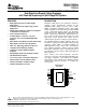
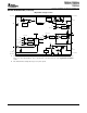
PWP PACKAGE
(TOP VIEW)
NC
V
IN1
V
IN1
MR1
MR2
EN
SEQ
GND
V
IN2
V
IN2
NC
V
OUT1
V
OUT1
V
SENSE1
/FB1
PG1
RESET
V
SENSE2
/FB2
V
OUT2
V
OUT2
NC
TPS70145, TPS70148
TPS70151, TPS70158
TPS70102
SLVS222D – DECEMBER 1999 – REVISED NOVEMBER 2004
Dual-Output Low-Dropout Voltage Regulators
with Power-Up Sequencing for Split-Voltage DSP Systems
• Dual Output Voltages for Split-Supply
TPS701xx family devices are designed to provide a
Applications
complete power management solution for the
TMS320™ DSP family, processor power, ASIC,
• Selectable Power-Up Sequencing for DSP
FPGA, and digital applications where dual output
Applications
voltage regulators are required. Easy programmability
• Output Current Range of 500mA on Regulator
of the sequencing function makes the TPS701xx
1 and 250mA on Regulator 2
family ideal for any TMS320 DSP applications with
• Fast Transient Response
power sequencing requirements. Differentiated fea-
tures, such as accuracy, fast transient response, SVS
• Voltage Options: 3.3V/2.5V, 3.3V/1.8V,
supervisory circuit, manual reset inputs, and an
3.3V/1.5V, 3.3V/1.2V, and Dual Adjustable
enable function, provide a complete system solution.
Outputs
The TPS701xx family of voltage regulators offers very
• Open Drain Power-On Reset with 120ms Delay
low dropout voltage and dual outputs with power-up
• Open Drain Power Good for Regulator 1
sequence control, which is designed primarily for
• Ultra Low 190µA (typ) Quiescent Current
DSP applications. These devices have extremely low
noise output performance without using any added
• 1µA Input Current During Standby
filter bypass capacitors and are designed to have a
• Low Noise: 65µV
RMS
Without Bypass
fast transient response and be stable with 10µF low
Capacitor
ESR capacitors.
• Quick Output Capacitor Discharge Feature
These devices have fixed 3.3V/2.5V, 3.3V/1.8V,
• Two Manual Reset Inputs
3.3V/1.5V, 3.3V/1.2V, and adjustable/adjustable volt-
• 2% Accuracy Over Load and Temperature
age options. Regulator 1 can support up to 500mA,
and regulator 2 can support up to 250mA. Separate
• Undervoltage Lockout (UVLO) Feature
voltage inputs allow the designer to configure the
• 20-Pin PowerPAD™ TSSOP Package
source power.
• Thermal Shutdown Protection
Please be aware that an important notice concerning availability, standard warranty, and use in critical applications of Texas
Instruments semiconductor products and disclaimers thereto appears at the end of this data sheet.
PowerPAD, TMS320 are trademarks of Texas Instruments.
All other trademarks are the property of their respective owners.
PRODUCTION DATA information is current as of publication date.
Copyright © 1999–2004, Texas Instruments Incorporated
Products conform to specifications per the terms of the Texas
Instruments standard warranty. Production processing does not
necessarily include testing of all parameters.