TPS70245, TPS70248 TPS70251, TPS70258 TPS70202 www.ti.com SLVS286E – JUNE 2000 – REVISED DECEMBER 2009 DUAL-OUTPUT, LOW DROPOUT VOLTAGE REGULATORS WITH INTEGRATED SVS FOR SPLIT VOLTAGE SYSTEMS FEATURES DESCRIPTION • The TPS702xx is a low dropout voltage regulator with integrated SVS (RESET, POR, or power on reset) and power good (PG) functions. These devices are capable of supplying 500mA and 250mA by regulator 1 and regulator 2 respectively. Quiescent current is typically 190μA at full load.
TPS70245, TPS70248 TPS70251, TPS70258 TPS70202 SLVS286E – JUNE 2000 – REVISED DECEMBER 2009 www.ti.com The TPS702xx family of voltage regulators offers very low dropout voltage and dual outputs. These devices have extremely low noise output performance without using any added filter bypass capacitors and are designed to have a fast transient response and be stable with 10μF low ESR capacitors. These devices have fixed 3.3V/2.5V, 3.3V/1.8V, 3.3V/1.5V, 3.3V/1.2V, and adjustable voltage options.
TPS70245, TPS70248 TPS70251, TPS70258 TPS70202 www.ti.com SLVS286E – JUNE 2000 – REVISED DECEMBER 2009 This integrated circuit can be damaged by ESD. Texas Instruments recommends that all integrated circuits be handled with appropriate precautions. Failure to observe proper handling and installation procedures can cause damage. ESD damage can range from subtle performance degradation to complete device failure.
TPS70245, TPS70248 TPS70251, TPS70258 TPS70202 SLVS286E – JUNE 2000 – REVISED DECEMBER 2009 www.ti.com DISSIPATION RATINGS PACKAGE AIR FLOW (CFM) TA ≤ +25°C DERATING FACTOR TA = +70°C TA = +85°C 0 3.067W 30.67mW/°C 1.687W 1.227W 250 4.115W 41.15mW/°C 2.265W 1.646W PWP (1) (1) This parameter is measured with the recommended copper heat sink pattern on a 4-layer PCB, 1 oz. copper on a 4-in by 4-in ground layer. For more information, refer to TI technical brief SLMA002.
TPS70245, TPS70248 TPS70251, TPS70258 TPS70202 www.ti.com SLVS286E – JUNE 2000 – REVISED DECEMBER 2009 ELECTRICAL CHARACTERISTICS Over recommended operating junction temperature range (TJ = –40°C to +125°C), VIN1 or VIN2 = VOUT(nom) + 1V, IO = 1mA, EN1 = 0V, EN2 = 0V, and CO = 33μF (unless otherwise noted). PARAMETER Reference voltage 1.2V Output Output voltage VO (1) , 1.5V Output (2) 1.8V Output 2.5V Output 3.3V Output TEST CONDITIONS 2.7V < VIN < 6V, TJ = +25°C FB connected to VO 2.
TPS70245, TPS70248 TPS70251, TPS70258 TPS70202 SLVS286E – JUNE 2000 – REVISED DECEMBER 2009 www.ti.com ELECTRICAL CHARACTERISTICS (continued) Over recommended operating junction temperature range (TJ = –40°C to +125°C), VIN1 or VIN2 = VOUT(nom) + 1V, IO = 1mA, EN1 = 0V, EN2 = 0V, and CO = 33μF (unless otherwise noted). PARAMETER TEST CONDITIONS MIN TYP MAX UNIT 1.0 1.3 95 98 %VOUT PG1/PG2 Terminal V(PGx) ≤ 0.
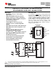
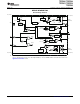
TPS70245, TPS70248 TPS70251, TPS70258 TPS70202 www.ti.com SLVS286E – JUNE 2000 – REVISED DECEMBER 2009 DEVICE INFORMATION Fixed Voltage Version VIN1 (2 Pins) VOUT1 (2 Pins) 2.5 V UVLO Comp 10 kW Current Sense + + GND VSENSE1 ENA_1 Thermal Shutdown Reference (see Note A) ENA_1 Vref FB1 Vref PG1 VSENSE1 - 0.95 x Vref + Rising Edge Deglitch VIN1 PG1 Comp MR RESET 120 ms Delay ENA_1 EN1 VSENSE2 - 0.
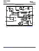
TPS70245, TPS70248 TPS70251, TPS70258 TPS70202 SLVS286E – JUNE 2000 – REVISED DECEMBER 2009 www.ti.com Adjustable Voltage Version VIN1 (2 Pins) VOUT1 (2 Pins) UVLO Comp Current Sense 2.5 V (see Note A) + GND FB1 ENA_1 + Thermal Shutdown Reference ENA_1 Vref Vref PG1 FB1 - 0.95 x Vref + Rising Edge Deglitch VIN1 PG1 Comp MR RESET 120 ms Delay ENA_1 EN1 PG2 Comp FB2 - 0.
TPS70245, TPS70248 TPS70251, TPS70258 TPS70202 www.ti.com SLVS286E – JUNE 2000 – REVISED DECEMBER 2009 RESET Timing Diagram VIN1 VUVLO VUVLO VRES (see Note A) t VRES (see Note A) MR Input t RESET Output Output Undefined 120 ms Delay 120 ms Delay Output Undefined t NOTE A: VRES is the minimum input voltage for a valid RESET. The symbol VRES is not currently listed within EIA or JEDEC standards for semiconductor symbology.
TPS70245, TPS70248 TPS70251, TPS70258 TPS70202 SLVS286E – JUNE 2000 – REVISED DECEMBER 2009 www.ti.com PG2 Timing Diagram (assuming VIN1 already powered up) VIN2 t VOUT2 VIT+ (see Note A) Threshold Voltage VIT(see Note A) t PG2 Output t NOTE A: VIT- trip voltage is typically 5% lower than the output voltage (95%VO). VIT- to VIT+ is the hysteresis voltage. TERMINAL FUNCTIONS TERMINAL NAME NO.
TPS70245, TPS70248 TPS70251, TPS70258 TPS70202 www.ti.com SLVS286E – JUNE 2000 – REVISED DECEMBER 2009 Detailed Description The TPS702xx low dropout regulator family provides dual regulated output voltages with independent enable functions. These devices provide fast transient response and high accuracy with small output capacitors, while drawing low quiescent current.
TPS70245, TPS70248 TPS70251, TPS70258 TPS70202 SLVS286E – JUNE 2000 – REVISED DECEMBER 2009 www.ti.com FB1 and FB2 FB1 and FB2 are input terminals used for adjustable-output devices and must be connected to the external feedback resistor divider. FB1 and FB2 connections should be as short as possible. It is essential to route them in such a way as to minimize or avoid noise pickup.
TPS70245, TPS70248 TPS70251, TPS70258 TPS70202 www.ti.
TPS70245, TPS70248 TPS70251, TPS70258 TPS70202 SLVS286E – JUNE 2000 – REVISED DECEMBER 2009 www.ti.com TYPICAL CHARACTERISTICS (continued) TPS70245 OUTPUT VOLTAGE vs OUTPUT CURRENT TPS70251 OUTPUT VOLTAGE vs JUNCTION TEMPERATURE 3.35 1.201 3.33 VO - Output Voltage - (V) 1.200 VO - Output Voltage - (V) VIN1 = 4.3 V VOUT1 VIN2 = 2.7 V TJ = +25°C VOUT2 1.199 1.198 1.197 1.196 IO = 500 mA 3.31 3.29 IO = 1 mA 3.27 3.25 1.195 0 0.05 0.2 0.1 0.15 I O - Output Current - (A) 3.23 -40 -25 -10 0.
TPS70245, TPS70248 TPS70251, TPS70258 TPS70202 www.ti.
TPS70245, TPS70248 TPS70251, TPS70258 TPS70202 SLVS286E – JUNE 2000 – REVISED DECEMBER 2009 www.ti.com TYPICAL CHARACTERISTICS (continued) OUTPUT SPECTRAL NOISE DENSITY vs FREQUENCY OUTPUT SPECTRAL NOISE DENSITY vs FREQUENCY 10 VIN1 = 4.3 V VOUT1 = 3.3 V IO = 10 mA Output Spectral Noise Density - mV/ÖHz Output Spectral Noise Density - mV/ÖHz 10 1 0.1 0.01 100 1k 10 k f - Frequency - Hz 1k 10 k f - Frequency - Hz Figure 12.
TPS70245, TPS70248 TPS70251, TPS70258 TPS70202 www.ti.com SLVS286E – JUNE 2000 – REVISED DECEMBER 2009 TYPICAL CHARACTERISTICS (continued) OUTPUT IMPEDANCE vs FREQUENCY OUTPUT IMPEDANCE vs FREQUENCY 100 CO = 33 mF IO = 500 mA VOUT1 = 3.3 V TJ = +25°C 10 ZO - Output Impednace - W ZO - Output Impednace - W 100 1 0.1 0.01 10 100 100 k 1k 10 k f - Frequency - Hz 1M 0.1 10 100 1k 10 k 100 k Figure 15. Figure 16.
TPS70245, TPS70248 TPS70251, TPS70258 TPS70202 SLVS286E – JUNE 2000 – REVISED DECEMBER 2009 www.ti.com TYPICAL CHARACTERISTICS (continued) DROPOUT VOLTAGE vs TEMPERATURE DROPOUT VOLTAGE vs TEMPERATURE 6 250 CO = 33 mF VIN1 = 3.2 V CO = 33 mF VIN1 = 3.2 V 5 200 Dropout Voltage - mV Dropout Voltage - mV IO = 500 mA 150 100 50 IO = 10 mA 4 3 2 1 IO = 0 mA 0 40 25 10 5 20 35 50 65 80 0 -40 -25 -10 95 110 125 T - Temperature - °C Figure 20.
TPS70245, TPS70248 TPS70251, TPS70258 TPS70202 www.ti.com SLVS286E – JUNE 2000 – REVISED DECEMBER 2009 TYPICAL CHARACTERISTICS (continued) IO - Output Current - mA LOAD TRANSIENT RESPONSE CO = 33 mF TJ = +25°C VOUT1 = 3.3 V 500 250 0 20 0 -20 0 0.2 0.4 0.6 0.8 1 1.2 1.4 1.6 1.8 2 DVO - Change in Output Voltage - mV Output Voltage - mV DVO - Change in IO - Output Current - mA LOAD TRANSIENT RESPONSE CO = 33 mF TJ = +25°C VOUT2 = 1.8 V 250 0 20 0 -20 0 0.2 0.4 0.6 0.
TPS70245, TPS70248 TPS70251, TPS70258 TPS70202 SLVS286E – JUNE 2000 – REVISED DECEMBER 2009 www.ti.com TYPICAL CHARACTERISTICS (continued) OUTPUT VOLTAGE AND ENABLE VOLTAGE vs TIME (START-UP) Enable Voltage (EN2) - V VOUT2 - Output Voltage Enable Voltage (EN1) - V VOUT1 - Output Voltage OUTPUT VOLTAGE AND ENABLE VOLTAGE vs TIME (START-UP) 3 2 VO = 3.3 V CO = 33 mF IO = 500 mA VOUT2 = Standby 1 0 5 0 0 0.2 0.4 0.6 0.8 1.0 1.2 1.4 1.6 1.8 2.0 VO = 1.
TPS70245, TPS70248 TPS70251, TPS70258 TPS70202 www.ti.com SLVS286E – JUNE 2000 – REVISED DECEMBER 2009 TYPICAL CHARACTERISTICS (continued) TYPICAL REGION OF STABILITY EQUIVALENT SERIES RESISTANCE(1) vs OUTPUT CURRENT 10 REGION OF INSTABILITY ESR - Equivalent Series Resistance - W ESR - Equivalent Series Resistance - W 10 TYPICAL REGION OF STABILITY EQUIVALENT SERIES RESISTANCE(1) vs OUTPUT CURRENT VO = 3.3 V CO = 10 mF TJ = 25°C 1 0.1 50 mW REGION OF INSTABILITY 0.01 REGION OF INSTABILITY VO = 3.
TPS70245, TPS70248 TPS70251, TPS70258 TPS70202 SLVS286E – JUNE 2000 – REVISED DECEMBER 2009 www.ti.com APPLICATION INFORMATION TPS702xxPWP (Fixed Output Option) Sequencing Timing Diagrams This section provides a number of timing diagrams showing how this device functions in different configurations. VIN VIN1 0.1 mF VSENSE1 Application condition: VIN1 and VIN2 are tied to the same fixed input voltage greater than VUVLO. PG2 is tied to MR.
TPS70245, TPS70248 TPS70251, TPS70258 TPS70202 www.ti.com SLVS286E – JUNE 2000 – REVISED DECEMBER 2009 Application condition: VIN1 and VIN2 are tied to the same fixed input voltage greater than VUVLO. MR is initially logic high but is eventually toggled. EN1 and EN2 are initially high; therefore, both regulators are off, and PG1 and PG2 are at logic low. Since VIN1 is greater than VUVLO and MR is at logic high, RESET is also at logic high. When EN2 is taken to logic low, VOUT2 turns on.
TPS70245, TPS70248 TPS70251, TPS70258 TPS70202 SLVS286E – JUNE 2000 – REVISED DECEMBER 2009 www.ti.com Application condition: VIN1 and VIN2 are tied to same fixed input voltage greater than VUVLO. PG1 is tied to MR. EN1 and EN2 are initially high; therefore, both regulators are off, and PG1 (tied to MR) and PG2 are at logic low. Since MR is at logic low, RESET is also at logic low. When EN2 is taken to logic low, VOUT2 turns on. Later, when EN1 is taken to logic low, VOUT1 turns on.
TPS70245, TPS70248 TPS70251, TPS70258 TPS70202 www.ti.com SLVS286E – JUNE 2000 – REVISED DECEMBER 2009 APPLICATION INFORMATION Input Capacitor For a typical application, an input bypass capacitor (0.1μF to 1μF) is recommended. This capacitor filters any high-frequency noise generated in the line. For fast transient conditions where droop at the input of the LDO may occur because of high inrush current, it is recommended to place a larger capacitor at the input as well.
TPS70245, TPS70248 TPS70251, TPS70258 TPS70202 SLVS286E – JUNE 2000 – REVISED DECEMBER 2009 www.ti.com Figure 38 shows the output capacitor and its parasitic impedances in a typical LDO output stage. Iout LDO + VESR RESR − Vin RLOAD Vout Cout Figure 38. LDO Output Stage with Parasitic Resistances ESR In steady state (dc state condition), the load current is supplied by the LDO (solid arrow) and the voltage across the capacitor is the same as the output voltage (V(CO) = VOUT).
TPS70245, TPS70248 TPS70251, TPS70258 TPS70202 www.ti.com SLVS286E – JUNE 2000 – REVISED DECEMBER 2009 IOUT VOUT 1 2 3 ESR 1 ESR 2 ESR 3 t1 t2 Figure 39. Correlation of Different ESRs and Their Influence on the Regulation of VO at a Load Step from Low-to-High Output Current Figure 39 also shows the impact of different ESRs on the output voltage. The left brackets show different levels of ESRs where number 1 displays the lowest and number 3 displays the highest ESR.
TPS70245, TPS70248 TPS70251, TPS70258 TPS70202 SLVS286E – JUNE 2000 – REVISED DECEMBER 2009 www.ti.com OUTPUT VOLTAGE PROGRAMMING GUIDE TPS70202 VI IN OUTPUT VOLTAGE R1 R2 UNIT 2.5 V 31.6 30.1 kW 3.3 V 51.1 30.1 kW 3.6 V 59.0 30.1 kW 0.1 mF >2.0 V OUT EN VO <0.7 V + R1 FB GND R2 Figure 40.
TPS70245, TPS70248 TPS70251, TPS70258 TPS70202 www.ti.com SLVS286E – JUNE 2000 – REVISED DECEMBER 2009 REVISION HISTORY NOTE: Page numbers for previous revisions may differ from page numbers in the current version. Changes from Revision D (December, 2007) to Revision E Page • Corrected typo in output current limit specification units ...................................................................................................... 5 • Deleted falling edge delay specification .....................
PACKAGE OPTION ADDENDUM www.ti.
PACKAGE OPTION ADDENDUM www.ti.com 3-Dec-2009 TBD: The Pb-Free/Green conversion plan has not been defined. Pb-Free (RoHS): TI's terms "Lead-Free" or "Pb-Free" mean semiconductor products that are compatible with the current RoHS requirements for all 6 substances, including the requirement that lead not exceed 0.1% by weight in homogeneous materials. Where designed to be soldered at high temperatures, TI Pb-Free products are suitable for use in specified lead-free processes.
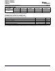
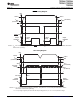
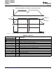
PACKAGE MATERIALS INFORMATION www.ti.com 14-Jul-2012 TAPE AND REEL INFORMATION *All dimensions are nominal Device Package Package Pins Type Drawing SPQ Reel Reel A0 Diameter Width (mm) (mm) W1 (mm) B0 (mm) K0 (mm) P1 (mm) TPS70202PWPR HTSSOP PWP 20 2000 330.0 16.4 TPS70245PWPR HTSSOP PWP 20 2000 330.0 TPS70248PWPR HTSSOP PWP 20 2000 330.0 TPS70251PWPR HTSSOP PWP 20 2000 TPS70258PWPR HTSSOP PWP 20 2000 6.95 7.1 1.6 8.0 16.0 Q1 16.4 6.95 7.1 1.6 8.0 16.
PACKAGE MATERIALS INFORMATION www.ti.com 14-Jul-2012 *All dimensions are nominal Device Package Type Package Drawing Pins SPQ Length (mm) Width (mm) Height (mm) TPS70202PWPR HTSSOP PWP 20 2000 367.0 367.0 38.0 TPS70245PWPR HTSSOP PWP 20 2000 367.0 367.0 38.0 TPS70248PWPR HTSSOP PWP 20 2000 367.0 367.0 38.0 TPS70251PWPR HTSSOP PWP 20 2000 367.0 367.0 38.0 TPS70258PWPR HTSSOP PWP 20 2000 367.0 367.0 38.
IMPORTANT NOTICE Texas Instruments Incorporated and its subsidiaries (TI) reserve the right to make corrections, enhancements, improvements and other changes to its semiconductor products and services per JESD46C and to discontinue any product or service per JESD48B. Buyers should obtain the latest relevant information before placing orders and should verify that such information is current and complete.