TPS70345, TPS70348 TPS70351, TPS70358 TPS70302 www.ti.com SLVS285H – AUGUST 2000 – REVISED APRIL 2010 DUAL-OUTPUT, LOW DROPOUT VOLTAGE REGULATORS WITH INTEGRATED SVS FOR SPLIT VOLTAGE SYSTEMS Check for Samples: TPS70345, TPS70348, TPS70351, TPS70358, TPS70302 FEATURES DESCRIPTION • The TPS703xx family of devices is designed to provide a complete power management solution for TI DSP, processor power, ASIC, FPGA, and digital applications where dual output voltage regulators are required.
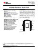
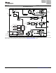
TPS70345, TPS70348 TPS70351, TPS70358 TPS70302 SLVS285H – AUGUST 2000 – REVISED APRIL 2010 www.ti.com TPS70351 PWP 5V VIN1 0.22 mF 3.3 V VOUT1 250 kW PG1 PG1 0.22 mF >2 V EN MR2 MR2 >2 V <0.7 V 250 kW RESET RESET EN <0.7 V MR1 VSENSE2 SEQ I/O 22 mF VSENSE1 VIN2 DSP MR1 >2 V <0.7 V 1.8 V VOUT2 Core 47 mF The TPS703xx family of voltage regulators offers very low dropout voltage and dual outputs with power up sequence control, designed primarily for DSP applications.
TPS70345, TPS70348 TPS70351, TPS70358 TPS70302 www.ti.com SLVS285H – AUGUST 2000 – REVISED APRIL 2010 This integrated circuit can be damaged by ESD. Texas Instruments recommends that all integrated circuits be handled with appropriate precautions. Failure to observe proper handling and installation procedures can cause damage. ESD damage can range from subtle performance degradation to complete device failure.
TPS70345, TPS70348 TPS70351, TPS70358 TPS70302 SLVS285H – AUGUST 2000 – REVISED APRIL 2010 www.ti.com DISSIPATION RATINGS PACKAGE AIR FLOW (CFM) TA ≤ +25°C DERATING FACTOR TA = +70°C TA = +85°C 0 3.067 W 30.67 mW/°C 1.687 W 1.227 W 250 4.115 W 41.15 mW/°C 2.265 W 1.646 W PWP (1) (1) This parameter is measured with the recommended copper heat sink pattern on a 4-layer PCB, 1 oz. copper on a 4-in by 4-in ground layer. For more information, refer to TI technical brief SLMA002.
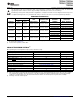
TPS70345, TPS70348 TPS70351, TPS70358 TPS70302 www.ti.com SLVS285H – AUGUST 2000 – REVISED APRIL 2010 ELECTRICAL CHARACTERISTICS Over recommended operating junction temperature range (TJ = –40°C to +125°C), VIN1 or VIN2 = VOUTX(nom) + 1V, IOUTX = 1mA, EN = 0V, COUT1 = 22mF, and COUT2 = 47mF (unless otherwise noted). PARAMETER TEST CONDITIONS 2.7 V < VIN < 6 V, TJ = +25°C FB connected to VO 2.7 V < VIN < 6 V, FB connected to VO 1.2 V output (VOUT2) 2.7 V < VIN < 6 V, TJ = +25°C 1.
TPS70345, TPS70348 TPS70351, TPS70358 TPS70302 SLVS285H – AUGUST 2000 – REVISED APRIL 2010 www.ti.com ELECTRICAL CHARACTERISTICS (continued) Over recommended operating junction temperature range (TJ = –40°C to +125°C), VIN1 or VIN2 = VOUTX(nom) + 1V, IOUTX = 1mA, EN = 0V, COUT1 = 22mF, and COUT2 = 47mF (unless otherwise noted). PARAMETER TEST CONDITIONS MIN TYP MAX UNIT 1.0 1.3 V 95 98 %VOUT PG Terminal V(PG1) ≤ 0.
TPS70345, TPS70348 TPS70351, TPS70358 TPS70302 www.ti.com SLVS285H – AUGUST 2000 – REVISED APRIL 2010 ELECTRICAL CHARACTERISTICS (continued) Over recommended operating junction temperature range (TJ = –40°C to +125°C), VIN1 or VIN2 = VOUTX(nom) + 1V, IOUTX = 1mA, EN = 0V, COUT1 = 22mF, and COUT2 = 47mF (unless otherwise noted).
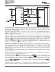
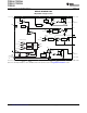
TPS70345, TPS70348 TPS70351, TPS70358 TPS70302 SLVS285H – AUGUST 2000 – REVISED APRIL 2010 www.ti.com DEVICE INFORMATION Adjustable Voltage Version VOUT1 (2 Pins) VIN1 (2 Pins) - UVLO1 Comp Current Sense FB1 ENA_1 + 2.5 V (see Note A) GND Reference Thermal Shutdown + ENA_1 Vref Vref PG1 FB1 - 0.95 x Vref + Rising Edge Deglitch VIN1 PG Comp MR2 Reset Comp VOUT2 UV Comp FB2 - 0.83 x Vref + FB1 - 0.83 x Vref + FB2 - 0.
TPS70345, TPS70348 TPS70351, TPS70358 TPS70302 www.ti.com SLVS285H – AUGUST 2000 – REVISED APRIL 2010 Fixed Voltage Version VOUT1 (2 Pins) VIN1 (2 Pins) - UVLO1 Comp 10 kW Current Sense VSENSE1 ENA_1 + 2.5 V (see Note A) GND Reference Thermal Shutdown + ENA_1 Vref FB1 Vref PG1 FB1 - 0.95 x Vref + Rising Edge Deglitch VIN1 PG Comp MR2 Reset Comp VOUT2 UV Comp FB2 - 0.83 x Vref + FB1 - 0.83 x Vref + FB2 - 0.95 x Vref + SEQ (see Note B) VIN1 Falling Edge Deglitch 2.
TPS70345, TPS70348 TPS70351, TPS70358 TPS70302 SLVS285H – AUGUST 2000 – REVISED APRIL 2010 www.ti.com RESET Timing Diagram with VIN1 Powered Up, MR1 and MR2 at Logic High VIN2 VRES (see Note A) VRES t VOUT2 VIT+ (see Note B) VIT +(see Note B) Threshold Voltage VIT(see Note B) VIT(see Note B) t RESET Output 120 ms Delay 120 ms Delay Output Undefined Output Undefined t NOTES: A. VRES is the minimum input voltage for a valid RESET.
TPS70345, TPS70348 TPS70351, TPS70358 TPS70302 www.ti.com SLVS285H – AUGUST 2000 – REVISED APRIL 2010 Detailed Description The TPS703xx low dropout regulator family provides dual regulated output voltages for DSP applications that require a high-performance power management solution. These devices provide fast transient response and high accuracy, while drawing low quiescent current. Programmable sequencing provides a power solution for DSPs without any external component requirements.
TPS70345, TPS70348 TPS70351, TPS70358 TPS70302 SLVS285H – AUGUST 2000 – REVISED APRIL 2010 www.ti.com FB1 and FB2 FB1 and FB2 are input terminals used for adjustable-output devices and must be connected to the external feedback resistor divider. FB1 and FB2 connections should be as short as possible. It is essential to route them in such a way as to minimize or avoid noise pickup.
TPS70345, TPS70348 TPS70351, TPS70358 TPS70302 www.ti.
TPS70345, TPS70348 TPS70351, TPS70358 TPS70302 SLVS285H – AUGUST 2000 – REVISED APRIL 2010 www.ti.com TYPICAL CHARACTERISTICS (continued) TPS70351 OUTPUT VOLTAGE vs JUNCTION TEMPERATURE TPS70351 OUTPUT VOLTAGE vs JUNCTION TEMPERATURE 1.834 3.354 VIN1 = 4.3 V VOUT1 VIN2 = 2.8 V VOUT2 1.824 3.314 VO - Output Voltage - V VO - Output Voltage - V 3.334 IO = 1 mA 3.294 IO = 1 A 3.274 3.254 1.814 IO = 2 A 1.804 IO = 1 mA 1.794 1.784 1.774 3.
TPS70345, TPS70348 TPS70351, TPS70358 TPS70302 www.ti.com SLVS285H – AUGUST 2000 – REVISED APRIL 2010 TYPICAL CHARACTERISTICS (continued) TPS70351 POWER-SUPPLY REJECTION RATIO vs FREQUENCY TPS70351 POWER-SUPPLY REJECTION RATIO vs FREQUENCY 20 30 0 VIN1 = 4.3 V VOUT1 = 3.
TPS70345, TPS70348 TPS70351, TPS70358 TPS70302 SLVS285H – AUGUST 2000 – REVISED APRIL 2010 www.ti.com TYPICAL CHARACTERISTICS (continued) OUTPUT SPECTRAL NOISE DENSITY vs FREQUENCY OUTPUT SPECTRAL NOISE DENSITY vs FREQUENCY 10 VIN1 = 4.3 V VOUT1 = 3.3 V COUT1 = 22 mF IO = 10 mA TJ = 25°C Output Spectral Noise Density - mV/ÖHz Output Spectral Noise Density - mV/ÖHz 10 1 0.1 0.01 100 1k 10 k f - Frequency - Hz 1k 10 k f - Frequency - Hz Figure 11.
TPS70345, TPS70348 TPS70351, TPS70358 TPS70302 www.ti.com SLVS285H – AUGUST 2000 – REVISED APRIL 2010 TYPICAL CHARACTERISTICS (continued) OUTPUT IMPEDANCE vs FREQUENCY OUTPUT IMPEDANCE vs FREQUENCY VOUT1 = 3.3 V IO = 1 A Co = 22 mF ZO - Output Impedance - W ZO - Output Impedance - W VOUT1 = 3.3 V IO = 10 mA Co = 22 mF 1 0.1 0.01 10 100 1k 10 k 100 k f - Frequency - Hz 1M 1 0.1 0.01 10 10 M Figure 15.
TPS70345, TPS70348 TPS70351, TPS70358 TPS70302 SLVS285H – AUGUST 2000 – REVISED APRIL 2010 www.ti.com TYPICAL CHARACTERISTICS (continued) DROPOUT VOLTAGE vs TEMPERATURE DROPOUT VOLTAGE vs TEMPERATURE 250 25 VOUT1 VIN1 = 3.2 V VOUT1 VIN1 = 3.
TPS70345, TPS70348 TPS70351, TPS70358 TPS70302 www.ti.com SLVS285H – AUGUST 2000 – REVISED APRIL 2010 TYPICAL CHARACTERISTICS (continued) 0.5 0 DVO - Change in Output Voltage - mV 50 0 50 100 0.2 0.4 0.6 0.8 1 1.2 t - Time - ms 1.4 1.6 1.8 0 50 0 50 0 0.2 0.4 0.6 0.8 1 1.2 1.4 1.6 t - Time - ms Figure 23. LINE TRANSIENT RESPONSE LINE TRANSIENT RESPONSE VOUT1 = 3.3 V IO = 1 A Co = 22 mF 4.3 50 0 50 0 1 Figure 22. 5.3 100 VOUT2 = 1.
TPS70345, TPS70348 TPS70351, TPS70358 TPS70302 SLVS285H – AUGUST 2000 – REVISED APRIL 2010 www.ti.com TYPICAL CHARACTERISTICS (continued) OUTPUT VOLTAGE AND ENABLE VOLTAGE vs TIME (START-UP) OUTPUT VOLTAGE AND ENABLE VOLTAGE vs TIME (START-UP) VO - Output Voltage - V 3 VOUT1 = 3.3 V IO = 1 A Co = 22 mF VIN1 = 4.3 V SEQ = Low 2 1 0 Enable Voltage - V Enable Voltage - V VO - Output Voltage - V 4 5 0 0 0.2 0.4 0.6 0.8 1 1.2 1.4 1.6 1.8 t - Time (Start-Up) - ms 2 2 1 0 VOUT2 = 1.
TPS70345, TPS70348 TPS70351, TPS70358 TPS70302 www.ti.com SLVS285H – AUGUST 2000 – REVISED APRIL 2010 TYPICAL CHARACTERISTICS (continued) TYPICAL REGION OF STABILITY EQUIVALENT SERIES RESISTANCE(1) vs OUTPUT CURRENT TYPICAL REGION OF STABILITY EQUIVALENT SERIES RESISTANCE(1) vs OUTPUT CURRENT 10 VOUT1 = 3.3 V Co = 22 mF ESR - Equivalent Series Resistance - W ESR - Equivalent Series Resistance - W 10 REGION OF INSTABILITY 1 0.1 50 mW 0.01 VOUT1 = 3.3 V Co = 220 mF REGION OF INSTABILITY 1 0.
TPS70345, TPS70348 TPS70351, TPS70358 TPS70302 SLVS285H – AUGUST 2000 – REVISED APRIL 2010 www.ti.com THERMAL INFORMATION Thermally-Enhanced TSSOP-24 (PWP— PowerPAD™) The thermally-enhanced PWP package is based on the 24-pin TSSOP, but includes a thermal pad [see Figure 33(c)] to provide an effective thermal contact between the IC and the printed wiring board (PWB). Traditionally, surface mount and power have been mutually exclusive terms.
TPS70345, TPS70348 TPS70351, TPS70358 TPS70302 www.ti.com SLVS285H – AUGUST 2000 – REVISED APRIL 2010 The thermal pad is directly connected to the substrate of the IC, which for the TPS703xx series is a secondary electrical connection to device ground. The heat-sink surface that is added to the PWP can be a ground plane or left electrically isolated. In TO220-type surface-mount packages, the thermal connection is also the primary electrical connection for a given terminal which is not always ground.
TPS70345, TPS70348 TPS70351, TPS70358 TPS70302 SLVS285H – AUGUST 2000 – REVISED APRIL 2010 www.ti.com 3.5 3.5 TA = 25°C TA = 55°C 300 ft/min 3 PD - Power Dissipation Limit - W PD - Power Dissipation Limit - W 3 150 ft/min 2.5 2 Natural Convection 1.5 1 0.5 0 300 ft/min 2.5 2 150 ft/min 1.5 Natural Convection 1 0.5 0 0.3 2 4 Copper Heatsink Size - cm 0 8 6 2 0 2 0.3 4 6 Copper Heatsink Size - cm (a) 8 2 (b) 3.5 TA = 105°C PD - Power Dissipation Limit - W 3 2.5 2 1.
TPS70345, TPS70348 TPS70351, TPS70358 TPS70302 www.ti.com SLVS285H – AUGUST 2000 – REVISED APRIL 2010 Figure 36 is an example of a thermally-enhanced PWB layout for use with the new PWP package. This board configuration was used in the thermal experiments that generated the power ratings shown in Figure 34 and Figure 35. As discussed earlier, copper has been added on the PWB to conduct heat away from the device. RqJA for this assembly is illustrated in Figure 34 as a function of heat-sink area.
TPS70345, TPS70348 TPS70351, TPS70358 TPS70302 SLVS285H – AUGUST 2000 – REVISED APRIL 2010 www.ti.com Comparing PD(total) with PD(max) reveals that the power dissipation in this example does not exceed the calculated limit. When it does, one of two corrective actions should be made: raising the power-dissipation limit by increasing the airflow or the heat-sink area, or lowering the internal power dissipation of the regulator by reducing the input voltage or the load current.
TPS70345, TPS70348 TPS70351, TPS70358 TPS70302 www.ti.com SLVS285H – AUGUST 2000 – REVISED APRIL 2010 APPLICATION INFORMATION MR1 and MR2 (tied to PG1) are at logic high, RESET is pulled to logic high after a 120 ms delay. When EN returns to a logic high, both devices power down and both PG1 (tied to MR2) and RESET return to logic low. Sequencing Timing Diagrams This section provides a number of timing diagrams showing how this device functions in different configurations.
TPS70345, TPS70348 TPS70351, TPS70358 TPS70302 SLVS285H – AUGUST 2000 – REVISED APRIL 2010 www.ti.com Application conditions not shown in block diagram: VIN1 and VIN2 are tied to the same fixed input voltage greater than VUVLO; SEQ is tied to logic high; PG1 is tied to MR2; MR1 is not used and is connected to VIN. TPS703xxPWP (Fixed Output Option) VI VIN1 0.22 mF Explanation of timing diagrams: EN is initially high; therefore, both regulators are off and PG1 and RESET are at logic low.
TPS70345, TPS70348 TPS70351, TPS70358 TPS70302 www.ti.com SLVS285H – AUGUST 2000 – REVISED APRIL 2010 Application conditions not shown in block diagram: VIN1 and VIN2 are tied to the same fixed input voltage greater than VUVLO; SEQ is tied to logic high; PG1 is tied to MR2; MR1 is initially at logic high but is eventually toggled. TPS703xxPWP (Fixed Output Option) VI VIN1 VOUT1 VOUT1 0.
TPS70345, TPS70348 TPS70351, TPS70358 TPS70302 SLVS285H – AUGUST 2000 – REVISED APRIL 2010 www.ti.com Application conditions not shown in block diagram: VIN1 and VIN2 are tied to the same fixed input voltage greater than VUVLO; SEQ is tied to logic high; PG1 is tied to MR2; MR1 is not used and is connected to VIN. TPS703xxPWP (Fixed Output Option) VI VIN1 0.22 mF Explanation of timing diagrams: EN is initially high; therefore, both regulators are off and PG1 and RESET are at logic low.
TPS70345, TPS70348 TPS70351, TPS70358 TPS70302 www.ti.com SLVS285H – AUGUST 2000 – REVISED APRIL 2010 Application conditions not shown in block diagram: VIN1 and VIN2 are tied to the same fixed input voltage greater than VUVLO; SEQ is tied to logic high; PG1 is tied to MR2; MR1 is not used and is connected to VIN. TPS703xxPWP (Fixed Output Option) VI VOUT1 VIN1 0.22 mF Explanation of timing diagrams: EN is initially high; therefore, both regulators are off and PG1 and RESET are at logic low.
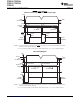
TPS70345, TPS70348 TPS70351, TPS70358 TPS70302 SLVS285H – AUGUST 2000 – REVISED APRIL 2010 www.ti.com APPLICATION INFORMATION Split Voltage DSP Application Figure 43 shows a typical application where the TPS70351 is powering up a DSP. In this application, by grounding the SEQ pin, VOUT1 (I/O) powers up first, and then VOUT2 (core). TPS70351 PWP 5V VIN1 0.22 mF 22 mF VSENSE1 MR2 0.22 mF >2 V EN I/O 250 kW PG1 PG1 VIN2 DSP 3.3 V VOUT1 MR2 250 kW RESET RESET MR1 EN MR1 <0.
TPS70345, TPS70348 TPS70351, TPS70358 TPS70302 www.ti.com SLVS285H – AUGUST 2000 – REVISED APRIL 2010 Figure 44 shows a typical application where the TPS70351 is powering up a DSP. In this application, by pulling up the SEQ pin, VOUT2 (core) powers up first, and then VOUT1 (I/O). TPS70351 PWP 5V VIN1 0.22 mF 22 mF VSENSE1 MR2 EN 250 kW MR2 250 kW 0.22 mF >2 V I/O PG1 PG1 VIN2 DSP 3.3 V VOUT1 RESET RESET MR1 EN MR1 <0.7 V VSENSE2 SEQ 1.
TPS70345, TPS70348 TPS70351, TPS70358 TPS70302 SLVS285H – AUGUST 2000 – REVISED APRIL 2010 www.ti.com Input Capacitor For a typical application, a ceramic input bypass capacitor (0.22 mF to 1 mF) is recommended to ensure device stability. This capacitor should be as close as possible to the input pin. Because of the impedance of the input supply, large transient currents cause the input voltage to droop. If this droop causes the input voltage to drop below the UVLO threshold, the device turns off.
TPS70345, TPS70348 TPS70351, TPS70358 TPS70302 www.ti.com SLVS285H – AUGUST 2000 – REVISED APRIL 2010 Programming the TPS70302 Adjustable LDO Regulator The output voltage of the TPS70302 adjustable regulators is programmed using external resistor dividers as shown in Figure 45. Resistors R1 and R2 should be chosen for approximately a 50 mA divider current. Lower value resistors can be used, but offer no inherent advantage and waste more power.
TPS70345, TPS70348 TPS70351, TPS70358 TPS70302 SLVS285H – AUGUST 2000 – REVISED APRIL 2010 www.ti.com REVISION HISTORY NOTE: Page numbers for previous revisions may differ from page numbers in the current version. Changes from Revision G (December 2009) to Revision H • Changed Tube transport media, quantity value from 70 to 60 in Ordering Information table ..............................................
PACKAGE OPTION ADDENDUM www.ti.
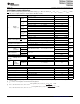
PACKAGE OPTION ADDENDUM www.ti.com Orderable Device 10-Jun-2014 Status (1) TPS70358PWPRG4 ACTIVE Package Type Package Pins Package Drawing Qty HTSSOP PWP 24 2000 Eco Plan Lead/Ball Finish MSL Peak Temp (2) (6) (3) Green (RoHS & no Sb/Br) CU NIPDAU Level-2-260C-1 YEAR Op Temp (°C) Device Marking (4/5) -40 to 125 PT70358 (1) The marketing status values are defined as follows: ACTIVE: Product device recommended for new designs.
PACKAGE OPTION ADDENDUM www.ti.
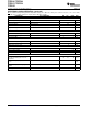
PACKAGE MATERIALS INFORMATION www.ti.com 14-Jul-2012 TAPE AND REEL INFORMATION *All dimensions are nominal Device Package Package Pins Type Drawing SPQ Reel Reel A0 Diameter Width (mm) (mm) W1 (mm) B0 (mm) K0 (mm) P1 (mm) TPS70302PWPR HTSSOP PWP 24 2000 330.0 16.4 TPS70345PWPR HTSSOP PWP 24 2000 330.0 TPS70348PWPR HTSSOP PWP 24 2000 330.0 TPS70351PWPR HTSSOP PWP 24 2000 TPS70358PWPR HTSSOP PWP 24 2000 6.95 8.3 1.6 8.0 16.0 Q1 16.4 6.95 8.3 1.6 8.0 16.
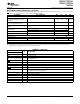
PACKAGE MATERIALS INFORMATION www.ti.com 14-Jul-2012 *All dimensions are nominal Device Package Type Package Drawing Pins SPQ Length (mm) Width (mm) Height (mm) TPS70302PWPR HTSSOP PWP 24 2000 367.0 367.0 38.0 TPS70345PWPR HTSSOP PWP 24 2000 367.0 367.0 38.0 TPS70348PWPR HTSSOP PWP 24 2000 367.0 367.0 38.0 TPS70351PWPR HTSSOP PWP 24 2000 367.0 367.0 38.0 TPS70358PWPR HTSSOP PWP 24 2000 367.0 367.0 38.
IMPORTANT NOTICE Texas Instruments Incorporated and its subsidiaries (TI) reserve the right to make corrections, enhancements, improvements and other changes to its semiconductor products and services per JESD46, latest issue, and to discontinue any product or service per JESD48, latest issue. Buyers should obtain the latest relevant information before placing orders and should verify that such information is current and complete.