
Datasheet


OUT
NC
FB/NC
IN
NC
GND
GND
1
2
3
6
5
4
3
2
4
51
FB/NC
GND
NC
OUT
IN
TPS714xx
www.ti.com
SBVS116C –DECEMBER 2008– REVISED MARCH 2011
ELECTRICAL CHARACTERISTICS
Over the operating junction temperature range (T
J
= –40°C to +125°C), V
IN
= V
OUT(NOM)
+ 1V, I
OUT
= 1mA, and C
OUT
= 1μF,
unless otherwise noted. The adjustable version is tested with V
OUT
= 2.8V. Typical values are at T
J
= +25°C.
TPS714xx
PARAMETER TEST CONDITIONS MIN TYP MAX UNIT
I
OUT
= 10mA 2.5 10
Input voltage range
(1)
V
IN
V
I
OUT
= 80mA 3 10
Output voltage range V
V
OUT
V
FB
8.8
(TPS71401)
Internal reference V
V
FB
1.12 1.20 1.24
(TPS71401)
TPS71433
Output voltage accuracy
(1)
over V
IN
, I
OUT
, 4.3V < V
IN
< 10V, 1mA ≤ I
OUT
≤ 80mA 3.135 3.3 3.465 V
and Temp
Output voltage
ΔV
OUT
/ΔV
IN
V
OUT
+ 1V < V
IN
≤ 10V 5 mV
line regulation
(1)
Load regulation ΔV
OUT
/ΔI
OUT
I
OUT
= 1mA to 80mA 30 mV
Feedback pin bias current I
FB BIAS
I
OUT
= 0mA, V
IN
= 3V to 10V, V
OUT
= 1.2V, 2 nA
Dropout voltage V
DO
I
OUT
= 80mA, V
IN
= V
OUT(NOM)
– 0.1V 670 1300 mV
Output current limit I
CL
V
OUT
= 0V 100 1100 mA
T
J
= –40°C to +85°C, 1mA ≤ I
OUT
≤ 80mA 3.2 4.2
Ground pin current I
GND
1mA ≤ I
OUT
≤ 80mA 3.2 5.8 μA
V
IN
= 10V, 1mA ≤ I
OUT
≤ 80mA 7.4
Power-supply ripple
PSRR f = 100kHz, C
OUT
= 10μF 60 dB
rejection
BW = 200Hz to 100kHz,
Output noise voltage V
IN
575 μVrms
C
OUT
= 10μF, I
OUT
= 50mA
(1) Minimum V
IN
= V
OUT
+ V
DO
, or the value shown for Input voltage, whichever is greater.
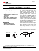
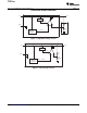
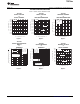
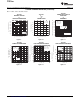
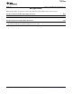
PIN CONFIGURATION
DRV PACKAGE
DCK PACKAGE
SON-6
SC70-5
(TOP VIEW)
(TOP VIEW)
Table 1. Pin Descriptions
TPS714xx
DCK DRV
NAME FIXED ADJ. FIXED ADJ. DESCRIPTION
FB/NC - 1 - 4 Adjustable version only. This pin is used to set the output voltage.
GND 2 2 3, Pad 3, Pad Ground
No connection. May be left open or tied to ground for improved thermal
NC 1,3 3 2, 4, 5 2, 5
performance.
IN 4 4 1 1 Unregulated input voltage.
Regulated output voltage. Any output capacitor ≥ 0.47μF can be used for
OUT 5 5 6 6
stability.
Copyright © 2008–2011, Texas Instruments Incorporated Submit Documentation Feedback 3