
Datasheet
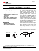


TPS71433
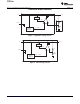
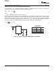
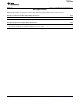
IN OUT
V
IN
V
OUT
C1
0.1 Fm
0.47 Fm
GND
P
D(max)
+
T
J
max * T
A
R
qJA
P
D
+
ǒ
V
IN
* V
OUT
Ǔ
I
OUT
TPS714xx
www.ti.com
SBVS116C –DECEMBER 2008– REVISED MARCH 2011
APPLICATION INFORMATION
The TPS714xx family of LDO regulators has been optimized for ultralow power applications such as the MSP430
microcontroller. Its ultralow supply current maximizes efficiency at light loads, and its high input voltage range
makes it suitable for supplies such as unconditioned solar panels.
Figure 15. Typical Application Circuit (Fixed Voltage Version)
External Capacitor Requirements
Although not required, a 0.047μF or larger input bypass capacitor, connected between IN and GND and located
close to the device, is recommended to improve transient response and noise rejection of the power supply as a
whole. A higher-value input capacitor may be necessary if large, fast-rise-time load transients are anticipated and
if the device is located several inches from the power source.
The TPS714xx requires an output capacitor connected between OUT and GND to stabilize the internal control
loop. Any capacitor (including ceramic and tantalum) that is greater than or equal to 0.47μF properly stabilizes
this loop.
Power Dissipation and Junction Temperature
To ensure reliable operation, worst-case junction temperature should not exceed +125°C. This restriction limits
the power dissipation that the regulator can manage in any given application. To ensure the junction temperature
is within acceptable limits, calculate the maximum allowable dissipation, P
D(MAX)
, and the actual dissipation, P
D
,
which must be less than or equal to P
D(max)
.
The maximum-power-dissipation limit is determined using Equation 1:
Where:
• T
J
max is the maximum allowable junction temperature.
• R
θJA
is the thermal resistance junction-to-ambient for the package (see the Power Dissipation Rating table).
• T
A
is the ambient temperature. (1)
The regulator dissipation is calculated using Equation 2:
(2)
Power dissipation resulting from quiescent current is negligible.
Regulator Protection
The TPS714xx PMOS-pass transistor has a built-in back diode that conducts reverse current when the input
voltage drops below the output voltage (for example, during power-down). Current is conducted from the output
to the input and is not internally limited. If extended reverse voltage operation is anticipated, external limiting
might be appropriate.
The TPS714xx features internal current limiting. During normal operation, the TPS714xx limits output current to
approximately 500mA. When current limiting engages, the output voltage scales back linearly until the
over-current condition ends. There is no internal thermal shutdown circuit in this device; therefore, care must be
taken not to exceed the power dissipation ratings of the package during a fault condition. This device does not
have undervoltage lockout; therefore, this constraint should be taken into consideration for specific applications.
Copyright © 2008–2011, Texas Instruments Incorporated Submit Documentation Feedback 7