
Datasheet


V
OUT
+ V
REF
ǒ
1 )
R1
R2
Ǔ
R1 +
ǒ
V
OUT
V
REF
* 1
Ǔ
R2
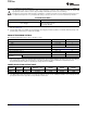
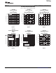
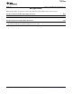
OUTPUTVOLTAGE
PROGRAMMINGGUIDE
OUTPUT
VOLTAGE
R1 R2
1.8V
2.8V
5.0V
392MW
1.07MW
2.55MW
806kW
806kW
806kW
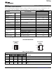
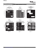
V
IN
FB
GND
IN
0.1 Fm
TPS71401
OUT
0.47 Fm
V
OUT
R1
R2
TPS714xx
SBVS116C –DECEMBER 2008– REVISED MARCH 2011
www.ti.com
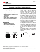
Programming the TPS71401 Adjustable LDO Regulator
The output voltage of the TPS71401 adjustable regulator is programmed using an external resistor divider as
shown in Figure 16. The output voltage is calculated using Equation 3:
(3)
where:
V
REF
= 1.20V typ (the internal reference voltage)
Resistors R1 and R2 should be chosen for approximately a 1.5μA divider current. Lower value resistors can be
used for improved noise performance, but the solution consumes more power. Higher resistor values should be
avoided because leakage current out of the FB pin across R1/R2 creates an offset voltage that artificially
increases the feedback voltage and thus erroneously decreases V
OUT
. The recommended design procedure is to
choose R2 = 1MΩ to set the divider current at 1.5μA, and then calculate R1 using Equation 4:
(4)
Figure 16. TPS71401 Adjustable LDO Regulator Programming
8 Submit Documentation Feedback Copyright © 2008–2011, Texas Instruments Incorporated