
Datasheet


1
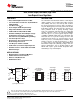
FEATURES DESCRIPTION
APPLICATIONS
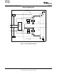
TPS718xx
TPS719xx
GND
EN1
EN2
OUT2
IN OUT1
V
IN
V
OUT
V
OUT
1 Fm
1 Fm
1 Fm
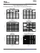
TypicalApplicationCircuit
2.7Vto6.5V 0.9Vto3.6V
0.9V 3.6V-
On
Off
On
Off
EN1
GND
GND
EN2
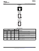
6
5
4
OUT1
IN
OUT2
1
2
3
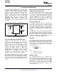
TPS718xx,TPS719xx
DRVPackage
2mmx2mmSON-6
(TopView)
OUT1
IN
OUT2
EN1
GND
EN2
A1
B1
C1
A2
B2
C2
TPS718Axx,TPS719Axx
YZCPackage
6-BALLWCSP
(TopView)
OUT1
IN
OUT2
EN1
GND
EN2
C2
B2
A2
C1
B1
A1
TPS718xx,TPS719xx
YZCPackage
6-BALLWCSP
(TopView)
TPS718xx
TPS719xx
www.ti.com
..................................................................................................................................................... SBVS088C – FEBRUARY 2007 – REVISED MAY 2008
Dual, 200mA Output, Low Noise, High PSRR
Low-Dropout Linear Regulators
23
• Dual, 200mA High-Performance LDOs
The TPS718xx and TPS719xx families of low-dropout
(LDO) regulators offer a high power-supply rejection
• Low Total Quiescent Current: 90 µ A with Both
ratio (PSRR), low noise, fast start-up, and excellent
LDOs Enabled
line and load transient responses while consuming a
• Low Noise: 70 µ V
RMS
/V
very low 90 µ A (typical) at no load ground current with
• Active Output Pulldown (TPS719xx)
both LDOs enabled. The TPS719xx also provides an
active pulldown circuit to quickly discharge output
• Independent Enables for Each LDO
loads. The TPS718xx and TPS719xx are stable with
• PSRR: 65dB at 1kHz, 45dB at 1MHz
ceramic capacitors and use an advanced BiCMOS
• Available in Multiple Fixed-Output Voltage
fabrication process to yield a typical dropout voltage
Combinations from 0.9V to 3.6V Using
of 230mV at 200mA output loads. The TPS718xx and
Innovative Factory EEPROM Programming
TPS719xx also use a precision voltage reference and
feedback loop to achieve 3% overall accuracy over all
• Fast Start-Up Time: 160 µ s
load, line, process, and temperature variations. Both
• Over-Current, Over-Temperature and
families of devices are fully specified from T
J
= – 40 ° C
Under-Voltage Protection
to +125 ° C and are offered in 2mm × 2mm SON-6 and
• Low Dropout: 230mV at 200mA
6-ball Wafer Chip-Scale (WCSP) packages that are
ideal for applications such as mobile handsets and
• Stable with 1 µ F Ceramic Output Capacitor
WLAN that require good thermal dissipation while
• Available in 2mm × 2mm SON-6 and 6-Ball
maintaining a very small footprint.
WCSP Packages
• Digital Cameras and Camera Modules
• Cellular Camera and TV Phones
• Wireless LAN, Bluetooth
®
• Handheld Products
1
Please be aware that an important notice concerning availability, standard warranty, and use in critical applications of
Texas Instruments semiconductor products and disclaimers thereto appears at the end of this data sheet.
2 Bluetooth is a registered trademark of Bluetooth SIG, Inc.
3 All other trademarks are the property of their respective owners.
PRODUCTION DATA information is current as of publication date.
Copyright © 2007 – 2008, Texas Instruments Incorporated
Products conform to specifications per the terms of the Texas
Instruments standard warranty. Production processing does not
necessarily include testing of all parameters.