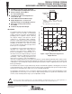
TPS7201Q, TPS7225Q, TPS7230Q TPS7233Q, TPS7248Q, TPS7250Q, TPS72xxY MICROPOWER LOW-DROPOUT (LDO) VOLTAGE REGULATORS SLVS102G – MARCH 1995 – REVISED JUNE 2000 D D D D D D D D, P, OR PW PACKAGE (TOP VIEW) Available in 5-V, 4.85-V, 3.3-V, 3.0-V, and 2.
TPS7201Q, TPS7225Q, TPS7230Q TPS7233Q, TPS7248Q, TPS7250Q, TPS72xxY MICROPOWER LOW-DROPOUT (LDO) VOLTAGE REGULATORS SLVS102G – MARCH 1995 – REVISED JUNE 2000 AVAILABLE OPTIONS TJ OUTPUT VOLTAGE (V) MIN – 55°C to 150°C TYP PACKAGED DEVICES MAX SMALL OUTLINE (D) PDIP (P) TSSOP (PW) CHIP FORM (Y) 4.9 5 5.1 TPS7250QD TPS7250QP TPS7250QPWR TPS7250Y 4.75 4.85 4.95 TPS7248QD TPS7248QP TPS7248QPWR TPS7248Y 3.23 3.3 3.37 TPS7233QD TPS7233QP TPS7233QPWR TPS7233Y 2.94 3 3.
TPS7201Q, TPS7225Q, TPS7230Q TPS7233Q, TPS7248Q, TPS7250Q, TPS72xxY MICROPOWER LOW-DROPOUT (LDO) VOLTAGE REGULATORS SLVS102G – MARCH 1995 – REVISED JUNE 2000 TPS72xx chip information These chips, when properly assembled, display characteristics similar to the TPS72xxQ. Thermal compression or ultrasonic bonding may be used on the doped aluminum bonding pads. The chips may be mounted with conductive epoxy or a gold-silicon preform.
TPS7201Q, TPS7225Q, TPS7230Q TPS7233Q, TPS7248Q, TPS7250Q, TPS72xxY MICROPOWER LOW-DROPOUT (LDO) VOLTAGE REGULATORS SLVS102G – MARCH 1995 – REVISED JUNE 2000 absolute maximum ratings over operating free-air temperature range (unless otherwise noted)Ĕ Input voltage rangeĕ, VI, PG, SENSE, EN . . . . . . . . . . . . . . . . . . . . . . . . . . . . . . . . . . . . . . . . . . . . – 0.3 V to 11 V Output current, IO . . . . . . . . . . . . . . . . . . . . . . . . . . . . . . . . . . . . . . . . . . . . . . . . .
TPS7201Q, TPS7225Q, TPS7230Q TPS7233Q, TPS7248Q, TPS7250Q, TPS72xxY MICROPOWER LOW-DROPOUT (LDO) VOLTAGE REGULATORS SLVS102G – MARCH 1995 – REVISED JUNE 2000 recommended operating conditions Input voltage, voltage VI† MIN MAX TPS7201Q 3 10 TPS7225Q 3.65 10 TPS7230Q 3.96 10 TPS7233Q 3.98 10 TPS7248Q 5.24 10 TPS7250Q 5.41 10 High-level input voltage at EN, VIH 2 Low-level input voltage at EN, VIL Output current, IO 0 UNIT V V 0.
TPS7201Q, TPS7225Q, TPS7230Q TPS7233Q, TPS7248Q, TPS7250Q, TPS72xxY MICROPOWER LOW-DROPOUT (LDO) VOLTAGE REGULATORS SLVS102G – MARCH 1995 – REVISED JUNE 2000 electrical characteristics, IO = 10 mA, EN = 0 V, CO = 4.7 µF (CSR† = 1 Ω), SENSE/FB shorted to OUT (unless otherwise noted) TEST CONDITIONS‡ PARAMETER Ground current (active mode) EN ≤ 0.
TPS7201Q, TPS7225Q, TPS7230Q TPS7233Q, TPS7248Q, TPS7250Q, TPS72xxY MICROPOWER LOW-DROPOUT (LDO) VOLTAGE REGULATORS SLVS102G – MARCH 1995 – REVISED JUNE 2000 TPS7201Q electrical characteristics, IO = 10 mA, VI = 3.5 V, EN = 0 V, CO = 4.7 µF (CSR† = 1 Ω), FB shorted to OUT at device leads (unless otherwise noted) TEST CONDITIONS‡ PARAMETER Reference voltage g ((measured at FB with OUT connected to FB) VI = 3.
TPS7201Q, TPS7225Q, TPS7230Q TPS7233Q, TPS7248Q, TPS7250Q, TPS72xxY MICROPOWER LOW-DROPOUT (LDO) VOLTAGE REGULATORS SLVS102G – MARCH 1995 – REVISED JUNE 2000 TPS7225Q electrical characteristics, IO = 10 mA, VI = 3.5 V, EN = 0 V, CO = 4.7 µF (CSR† = 1 Ω), SENSE shorted to OUT (unless otherwise noted) TEST CONDITIONS‡ PARAMETER TJ Output voltage VI = 3.5 V, 3.5 V ≤ VI ≤ 10 V, IO = 10 mA 5 mA ≤ IO ≤ 250 mA Dropout voltage IO = 250 mA, mA VI = 2 2.
TPS7201Q, TPS7225Q, TPS7230Q TPS7233Q, TPS7248Q, TPS7250Q, TPS72xxY MICROPOWER LOW-DROPOUT (LDO) VOLTAGE REGULATORS SLVS102G – MARCH 1995 – REVISED JUNE 2000 TPS7230Q electrical characteristics, IO = 10 mA, VI = 4 V, EN = 0 V, CO = 4.7 µF (CSR† = 1 Ω), SENSE shorted to OUT (unless otherwise noted) TEST CONDITIONS‡ PARAMETER Output voltage TJ VI = 4 V, 4 V ≤ VI ≤ 10 V, IO = 10 mA 5 mA ≤ IO ≤ 250 mA IO = 100 mA, mA VI = 2 2.97 97 V Dropout voltage IO = 250 mA, mA VI = 2 2.
TPS7201Q, TPS7225Q, TPS7230Q TPS7233Q, TPS7248Q, TPS7250Q, TPS72xxY MICROPOWER LOW-DROPOUT (LDO) VOLTAGE REGULATORS SLVS102G – MARCH 1995 – REVISED JUNE 2000 TPS7233Q electrical characteristics, IO = 10 mA, VI = 4.3 V, EN = 0 V, CO = 4.7 µF (CSR† = 1 Ω), SENSE shorted to OUT (unless otherwise noted) TEST CONDITIONS‡ PARAMETER Output voltage TJ VI = 4.3 V, 4.3 V ≤ VI ≤ 10 V, IO = 10 mA 5 mA ≤ IO ≤ 250 mA IO = 10 mA, mA VI = 3 3.23 23 V IO = 100 mA, mA VI = 3 3.
TPS7201Q, TPS7225Q, TPS7230Q TPS7233Q, TPS7248Q, TPS7250Q, TPS72xxY MICROPOWER LOW-DROPOUT (LDO) VOLTAGE REGULATORS SLVS102G – MARCH 1995 – REVISED JUNE 2000 TPS7248Q electrical characteristics, IO = 10 mA, VI = 5.85 V, EN = 0 V, CO = 4.7 µF (CSR† = 1 Ω), SENSE shorted to OUT (unless otherwise noted) TEST CONDITIONS‡ PARAMETER Output voltage TJ VI = 5.85 V, 5.85 V ≤ VI ≤ 10 V, IO = 10 mA 5 mA ≤ IO ≤ 250 mA IO = 10 mA mA, VI = 4 4.75 75 V IO = 100 mA, mA VI = 4 4.
TPS7201Q, TPS7225Q, TPS7230Q TPS7233Q, TPS7248Q, TPS7250Q, TPS72xxY MICROPOWER LOW-DROPOUT (LDO) VOLTAGE REGULATORS SLVS102G – MARCH 1995 – REVISED JUNE 2000 TPS7250Q electrical characteristics, IO = 10 mA, VI = 6 V, EN = 0 V, CO = 4.7 µF (CSR† = 1 Ω), SENSE shorted to OUT (unless otherwise noted) TEST CONDITIONS‡ PARAMETER Output voltage VI = 6 V, 6 V ≤ VI ≤ 10 V, IO = 10 mA 5 mA ≤ IO ≤ 250 mA IO = 10 mA mA, VI = 4 4.88 88 V IO = 100 mA, mA VI = 4 4.88 88 V mA IO = 250 mA, 88 V VI = 4 4.
TPS7201Q, TPS7225Q, TPS7230Q TPS7233Q, TPS7248Q, TPS7250Q, TPS72xxY MICROPOWER LOW-DROPOUT (LDO) VOLTAGE REGULATORS SLVS102G – MARCH 1995 – REVISED JUNE 2000 electrical characteristics, IO = 10 mA, EN = 0 V, CO = 4.7 µF (CSR† = 1 Ω), TJ = 25°C, SENSE/FB shorted to OUT (unless otherwise noted) TEST CONDITIONS‡ PARAMETER Ground current (active mode) EN ≤ 0.5 V, 0 mA ≤ IO ≤ 250 mA VI = VO + 1 V, Output current limit threshold VO = 0 V, VI = 10 V MIN TPS72xxY TYP MAX UNIT µA 180 0.
TPS7201Q, TPS7225Q, TPS7230Q TPS7233Q, TPS7248Q, TPS7250Q, TPS72xxY MICROPOWER LOW-DROPOUT (LDO) VOLTAGE REGULATORS SLVS102G – MARCH 1995 – REVISED JUNE 2000 electrical characteristics, IO = 10 mA, EN = 0 V, CO = 4.7 µF (CSR† = 1 Ω), TJ = 25°C, FB shorted to OUT at device leads (unless otherwise noted) TEST CONDITIONS‡ PARAMETER TPS7225Y MIN TYP MAX UNIT Output voltage VI = 3.5 V, IO = 10 mA 2.5 V Dropout voltage VI = 2.97 V, IO = 250 mA 560 mV Pass-element series resistance (2.
TPS7201Q, TPS7225Q, TPS7230Q TPS7233Q, TPS7248Q, TPS7250Q, TPS72xxY MICROPOWER LOW-DROPOUT (LDO) VOLTAGE REGULATORS SLVS102G – MARCH 1995 – REVISED JUNE 2000 electrical characteristics, IO = 10 mA, EN = 0 V, CO = 4.7 µF (CSR† = 1 Ω), TJ = 25°C, SENSE shorted to OUT (unless otherwise noted) TEST CONDITIONS‡ PARAMETER Output voltage TPS7230Y MIN TYP VI = 4 V, VI = 2.97 V, IO = 10 mA IO = 100 mA VI = 2.97 V, (2.97 V – VO)/IO, IO = 250 mA IO = 250 mA VI = 2.
TPS7201Q, TPS7225Q, TPS7230Q TPS7233Q, TPS7248Q, TPS7250Q, TPS72xxY MICROPOWER LOW-DROPOUT (LDO) VOLTAGE REGULATORS SLVS102G – MARCH 1995 – REVISED JUNE 2000 electrical characteristics, IO = 10 mA, EN = 0 V, CO = 4.7 µF (CSR† = 1 Ω), TJ = 25°C, SENSE shorted to OUT (unless otherwise noted) (continued) TEST CONDITIONS‡ PARAMETER Output voltage TPS7248Y MIN TYP VI = 5.85 V, VI = 4.75 V, IO = 10 mA IO = 10 mA VI = 4.75 V, VI = 4.75 V, IO = 100 mA IO = 250 mA 216 (4.75 V – VO)/IO, IO = 250 mA VI = 4.
TPS7201Q, TPS7225Q, TPS7230Q TPS7233Q, TPS7248Q, TPS7250Q, TPS72xxY MICROPOWER LOW-DROPOUT (LDO) VOLTAGE REGULATORS SLVS102G – MARCH 1995 – REVISED JUNE 2000 TYPICAL CHARACTERISTICS Table of Graphs FIGURE vs Output current 5 vs Input voltage 6 IQ Quiescent current ∆IQ† Change in quiescent current vs Free-air temperature 7 VDO ∆VDO Dropout voltage vs Output current 8 Change in dropout voltage vs Free-air temperature 9 VDO rDS(on) Dropout voltage (TPS7201 only) vs Output current 10 Pass-
TPS7201Q, TPS7225Q, TPS7230Q TPS7233Q, TPS7248Q, TPS7250Q, TPS72xxY MICROPOWER LOW-DROPOUT (LDO) VOLTAGE REGULATORS SLVS102G – MARCH 1995 – REVISED JUNE 2000 TYPICAL CHARACTERISTICS QUIESCENT CURRENT vs OUTPUT CURRENT QUIESCENT CURRENT vs INPUT VOLTAGE 230 250 TA = 25°C TPS7233 200 210 200 TPS7233 VI = 10 V 190 TPS7250 VI = 10 V 180 TPS7248 VI = 5.85 V I Q – Quiescent Current – µ A I Q – Quiescent Current – µ A 220 170 TPS7250 VI = 6.0 V 160 150 150 TPS7201 With VO Programmed to 2.
TPS7201Q, TPS7225Q, TPS7230Q TPS7233Q, TPS7248Q, TPS7250Q, TPS72xxY MICROPOWER LOW-DROPOUT (LDO) VOLTAGE REGULATORS SLVS102G – MARCH 1995 – REVISED JUNE 2000 TYPICAL CHARACTERISTICS TPS7201 DROPOUT VOLTAGE vs OUTPUT CURRENT CHANGE IN DROPOUT VOLTAGE vs FREE-AIR TEMPERATURE 1.6 0.04 VI = 2.4 V† 1.4 TPS7230 0.03 VDO – Dropout Voltage – V TPS7233 0.02 0.01 TPS7248/TPS7250 0 – 0.01 – 0.02 1.2 VI = 2.9 V 1 VI = 2.6 V† VI = 3.2 V VI = 3.9 V 0.8 VI = 5.9 V 0.6 VI = 9.65 V 0.4 0.2 – 0.03 – 0.
TPS7201Q, TPS7225Q, TPS7230Q TPS7233Q, TPS7248Q, TPS7250Q, TPS72xxY MICROPOWER LOW-DROPOUT (LDO) VOLTAGE REGULATORS SLVS102G – MARCH 1995 – REVISED JUNE 2000 TYPICAL CHARACTERISTICS OUTPUT VOLTAGE vs INPUT VOLTAGE LINE REGULATION 5.5 25 5 TPS7250 TPS7248 4.5 ∆VO – Output Voltage – V ∆VO – Change in Output Voltage – mV TA = 25°C IO = 250 mA 4 3.5 TPS7233 3 2.5 2 TPS7201 With VO Programmed to 2.5 V 1.5 1 15 TPS7201 With VO Programmed to 2.
TPS7201Q, TPS7225Q, TPS7230Q TPS7233Q, TPS7248Q, TPS7250Q, TPS72xxY MICROPOWER LOW-DROPOUT (LDO) VOLTAGE REGULATORS SLVS102G – MARCH 1995 – REVISED JUNE 2000 TYPICAL CHARACTERISTICS MINIMUM INPUT VOLTAGE FOR VALID PG vs FREE-AIR TEMPERATURE POWER-GOOD (PG) ON-RESISTANCE vs INPUT VOLTAGE 1.3 VI – Minimum Input Voltage for Valid PG TA = 25°C 10 1 1.125 1.12 1.115 1.11 1.105 ÁÁ 1.095 – 40 – 20 0 1.5 2 2.5 3 3.5 4 4.
TPS7201Q, TPS7225Q, TPS7230Q TPS7233Q, TPS7248Q, TPS7250Q, TPS72xxY MICROPOWER LOW-DROPOUT (LDO) VOLTAGE REGULATORS SLVS102G – MARCH 1995 – REVISED JUNE 2000 TYPICAL CHARACTERISTICS LOAD TRANSIENT RESPONSE 200 100 0 TA = 25°C VI = 6 V CI = 0 CO = 4.7 µF (CSR = 1 Ω) – 100 – 200 105 55 5 0 100 200 300 400 500 I O – Output Current – mA ∆VO – Change in Output Voltage – mV TPS7201 (WITH VO PROGRAMMED TO 2.5 V), TPS7233 t – Time – µs Figure 20 200 100 0 TA = 25°C VI = 6 V CI = 0 CO = 4.
TPS7201Q, TPS7225Q, TPS7230Q TPS7233Q, TPS7248Q, TPS7250Q, TPS72xxY MICROPOWER LOW-DROPOUT (LDO) VOLTAGE REGULATORS SLVS102G – MARCH 1995 – REVISED JUNE 2000 TPS7201 WITH VO PROGRAMMED TO 2.5 V LINE TRANSIENT RESPONSE 100 50 0 – 50 – 100 TA = 25°C CI = 0 CO = 4.7 µF (CSR = 1 Ω) 6.5 6.25 6 0 100 200 300 VI – Input Voltage – V ∆VO – Change in Output Voltage – mV TYPICAL CHARACTERISTICS 400 t – Time – µs Figure 22 200 100 0 – 50 TA = 25°C CI = 0 CO = 4.7 µF (CSR = 1 Ω) – 100 6.5 6.
TPS7201Q, TPS7225Q, TPS7230Q TPS7233Q, TPS7248Q, TPS7250Q, TPS72xxY MICROPOWER LOW-DROPOUT (LDO) VOLTAGE REGULATORS SLVS102G – MARCH 1995 – REVISED JUNE 2000 TYPICAL CHARACTERISTICS 100 50 0 – 50 TA = 25°C CI = 0 CO = 4.7 µF (CSR = 1 Ω) – 100 6.5 6.
TPS7201Q, TPS7225Q, TPS7230Q TPS7233Q, TPS7248Q, TPS7250Q, TPS72xxY MICROPOWER LOW-DROPOUT (LDO) VOLTAGE REGULATORS SLVS102G – MARCH 1995 – REVISED JUNE 2000 TYPICAL CHARACTERISTICS TYPICAL REGIONS OF STABILITY TYPICAL REGIONS OF STABILITY COMPENSATION SERIES RESISTANCE (CSR)† vs OUTPUT CURRENT COMPENSATION SERIES RESISTANCE (CSR)† vs ADDED CERAMIC CAPACITANCE 100 CSR – Compensation Series Resistance – Ω CSR – Compensation Series Resistance – Ω 100 Region of Instability 10 1 TA = 25°C VI = VO + 1 V
TPS7201Q, TPS7225Q, TPS7230Q TPS7233Q, TPS7248Q, TPS7250Q, TPS72xxY MICROPOWER LOW-DROPOUT (LDO) VOLTAGE REGULATORS SLVS102G – MARCH 1995 – REVISED JUNE 2000 APPLICATION INFORMATION The design of the TPS72xx family of low-dropout (LDO) regulators is based on the higher-current TPS71xx family.
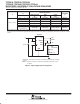
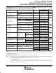
TPS7201Q, TPS7225Q, TPS7230Q TPS7233Q, TPS7248Q, TPS7250Q, TPS72xxY MICROPOWER LOW-DROPOUT (LDO) VOLTAGE REGULATORS SLVS102G – MARCH 1995 – REVISED JUNE 2000 APPLICATION INFORMATION TPS72xx (see Note A) 5 VI IN PG 6 PG 1 250 kΩ SENSE IN OUT C1 0.1 µF 2 4 OUT EN 7 VO 8 + GND 3 10 µF CSR = 1 Ω NOTE A: TPS7225, TPS7230, TPS7233, TPS7248, TPS7250 (fixed-voltage options). Figure 31. Typical Application Circuit external capacitor requirements Although not required, a 0.047-µF to 0.
TPS7201Q, TPS7225Q, TPS7230Q TPS7233Q, TPS7248Q, TPS7250Q, TPS72xxY MICROPOWER LOW-DROPOUT (LDO) VOLTAGE REGULATORS SLVS102G – MARCH 1995 – REVISED JUNE 2000 APPLICATION INFORMATION VI = VO + 1 V VO 1→ IO = 85 mA IO = 5 mA 2→ Ch1 Ch 2 50 mV 50 mA 100 µs/div Figure 32. Load Transient Response (CSR total = 1.7 Ω), TPS7248Q A partial listing of surface-mount capacitors usable with the TPS72xx family is provided below.
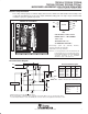
TPS7201Q, TPS7225Q, TPS7230Q TPS7233Q, TPS7248Q, TPS7250Q, TPS72xxY MICROPOWER LOW-DROPOUT (LDO) VOLTAGE REGULATORS SLVS102G – MARCH 1995 – REVISED JUNE 2000 APPLICATION INFORMATION output voltage programming The output voltage of the TPS7201 adjustable regulator is programmed using an external resistor divider as shown in Figure 33. The output voltage is calculated using: V O ǒ Ǔ + Vref @ 1 ) R1 R2 (1) Where: Vref = 1.
TPS7201Q, TPS7225Q, TPS7230Q TPS7233Q, TPS7248Q, TPS7250Q, TPS72xxY MICROPOWER LOW-DROPOUT (LDO) VOLTAGE REGULATORS SLVS102G – MARCH 1995 – REVISED JUNE 2000 APPLICATION INFORMATION power dissipation and junction temperature Specified regulator operation is assured to a junction temperature of 125°C; the maximum junction temperature allowable to avoid damaging the device is 150°C. These restrictions limit the power dissipation that the regulator can handle in any given application.
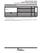
PACKAGE OPTION ADDENDUM www.ti.
PACKAGE OPTION ADDENDUM www.ti.
PACKAGE OPTION ADDENDUM www.ti.
PACKAGE OPTION ADDENDUM www.ti.com 11-Apr-2013 (1) The marketing status values are defined as follows: ACTIVE: Product device recommended for new designs. LIFEBUY: TI has announced that the device will be discontinued, and a lifetime-buy period is in effect. NRND: Not recommended for new designs. Device is in production to support existing customers, but TI does not recommend using this part in a new design. PREVIEW: Device has been announced but is not in production.
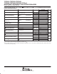
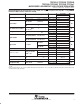
PACKAGE MATERIALS INFORMATION www.ti.com 26-Jan-2013 TAPE AND REEL INFORMATION *All dimensions are nominal Device Package Package Pins Type Drawing SPQ Reel Reel A0 Diameter Width (mm) (mm) W1 (mm) B0 (mm) K0 (mm) P1 (mm) W Pin1 (mm) Quadrant TPS7201QDR SOIC D 8 2500 330.0 12.4 6.4 5.2 2.1 8.0 12.0 Q1 TPS7201QPWR TSSOP PW 8 2000 330.0 12.4 7.0 3.6 1.6 8.0 12.0 Q1 TPS7225QDR SOIC D 8 2500 330.0 12.4 6.4 5.2 2.1 8.0 12.
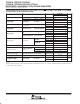
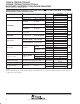
PACKAGE MATERIALS INFORMATION www.ti.com 26-Jan-2013 *All dimensions are nominal Device Package Type Package Drawing Pins SPQ Length (mm) Width (mm) Height (mm) TPS7201QDR SOIC D 8 2500 367.0 367.0 35.0 TPS7201QPWR TSSOP PW 8 2000 367.0 367.0 35.0 TPS7225QDR SOIC D 8 2500 367.0 367.0 35.0 TPS7225QPWR TSSOP PW 8 2000 367.0 367.0 35.0 TPS7230QPWR TSSOP PW 8 2000 367.0 367.0 35.0 TPS7233QDR SOIC D 8 2500 367.0 367.0 35.
IMPORTANT NOTICE Texas Instruments Incorporated and its subsidiaries (TI) reserve the right to make corrections, enhancements, improvements and other changes to its semiconductor products and services per JESD46, latest issue, and to discontinue any product or service per JESD48, latest issue. Buyers should obtain the latest relevant information before placing orders and should verify that such information is current and complete.