
Datasheet

TPS7201Q, TPS7225Q, TPS7230Q
TPS7233Q, TPS7248Q, TPS7250Q, TPS72xxY
MICROPOWER LOW-DROPOUT (LDO) VOLTAGE REGULATORS
SLVS102G – MARCH 1995 – REVISED JUNE 2000
3
POST OFFICE BOX 655303 • DALLAS, TEXAS 75265
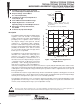
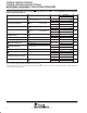
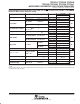
TPS72xx chip information
These chips, when properly assembled, display characteristics similar to the TPS72xxQ. Thermal compression
or ultrasonic bonding may be used on the doped aluminum bonding pads. The chips may be mounted with
conductive epoxy or a gold-silicon preform.
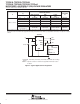
(6)
(4)
(3)
(7)
(2)
(1)
GND
FB
OUT
PG
IN
EN
TPS72xx
57
69
CHIP THICKNESS: 15 MILS TYPICAL
BONDING PADS: 4 × 4 MILS MINIMUM
T
J
max = 150°C
TOLERANCES ARE ±10%.
ALL DIMENSIONS ARE IN MILS.
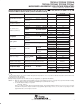
(6)
(7)
(2)
(5)
(4)
(3)
(1)
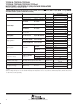
BONDING PAD ASSIGNMENTS
SENSE
(5)
NOTE A. For most applications, OUT and SENSE should
be tied together as close as possible to the device;
for other implementations, refer to the SENSE-pin
connection discussion in the application
information section of this data sheet.
7
6
5
4
1
2
3
†
Fixed-voltage options only (TPS7225, TPS7230,
TPS7233, TPS7248, and TPS7250)
‡
Adjustable version only (TPS7201)
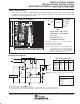
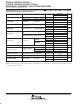
functional block diagram
_
+
V
ref
= 1.188 V
OUT
SENSE
¶
/FB
EN
IN
GND
R1
R2
PG
_
+
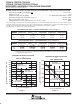
TPS7201
TPS7225
TPS7230
TPS7233
TPS7248
TPS7250
DEVICE
UNITR1 R2
0
257
357
420
726
756
∞
233
233
233
233
233
Ω
kΩ
kΩ
kΩ
kΩ
kΩ
RESISTOR DIVIDER OPTIONS
§
Switch positions are shown with EN
low (active).
¶
For most applications, SENSE should be externally connected to OUT as close as possible to the device.
For other implementations, refer to the SENSE-pin connection discussion in application information section.
NOTE A: Resistors are nominal values only.
1.12 V
§
§§
MOS transistors
Bilpolar transistors
Diodes
Capacitors
Resistors
COMPONENT COUNT
108
41
4
15
75