
Datasheet

TPS7201Q, TPS7225Q, TPS7230Q
TPS7233Q, TPS7248Q, TPS7250Q, TPS72xxY
MICROPOWER LOW-DROPOUT (LDO) VOLTAGE REGULATORS
SLVS102G – MARCH 1995 – REVISED JUNE 2000
7
POST OFFICE BOX 655303 • DALLAS, TEXAS 75265
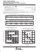
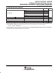
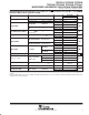
TPS7201Q electrical characteristics, I
O
= 10 mA, V
I
= 3.5 V, EN = 0 V, C
O
= 4.7 µF (CSR
†
= 1 Ω), FB
shorted to OUT at device leads (unless otherwise noted)
PARAMETER
TEST CONDITIONS
‡
T
J
TPS7201Q
UNIT
PARAMETER
TEST
CONDITIONS
‡
T
J
MIN TYP MAX
UNIT
Reference voltage (measured
V
I
= 3.5 V, I
O
= 10 mA 25°C 1.188 V
g(
at FB with OUT connected to
FB)
3 V ≤ V
I
≤ 10 V,
See Note 2
5 mA ≤ I
O
≤ 250 mA,
–40°C to 125°C 1.152 1.224 V
Reference voltage
temperature coefficient
–40°C to 125°C 31 75 ppm/°C
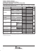
V
I
= 2.4 V,
§
50 µA ≤ I
O
≤ 100 mA 25°C 2.1
V
I
= 2.4 V,
§
100 mA ≤ I
O
≤ 200 mA 25°C 2.9
Pass-element series
V
I
=29V
50 µA ≤ I
O
≤ 250 mA
25°C 1.6 2.7
Ω
resistance (see Note 3)
V
I
=
2
.
9
V
,
50
µ
A
≤
I
O
≤
250
mA
–40°C to 125°C 4.5
Ω
V
I
= 3.9 V, 50 µA ≤ I
O
≤ 250 mA 25°C 1
V
I
= 5.9 V, 50 µA ≤ I
O
≤ 250 mA 25°C 0.8
In
p
ut regulation
V
I
= 3 V to 10 V, 50
µ
A ≤ I
O
≤ 250 mA,
25°C 23
mV
Inp
u
t
reg
u
lation
I
,
See Note 2
µ
O
,
–40°C to 125°C 36
mV
I
O
= 5 mA to 250 mA, 3 V ≤ V
I
≤ 10 V,
25°C 15 25
Out
p
ut regulation
O
,
See Note 2
I
,
–40°C to 125°C 36
mV
O
u
tp
u
t
reg
u
lation
I
O
= 50 µA to 250 mA, 3 V ≤ V
I
≤ 10 V,
25°C 17 27
mV
O
µ ,
See Note 2
I
,
–40°C to 125°C 43
I
O
=50µA
25°C 49 60
Ri
pp
le rejection
f = 120 Hz
I
O
=
50
µ
A
–40°C to 125°C 32
dB
Ripple
rejection
f
=
120
H
z
I
O
= 250 mA,
25°C 45 50
dB
O
,
See Note 2
–40°C to 125°C 30
Output noise spectral density f = 120 Hz 25°C 2
µV/√Hz
10 H ≤ f ≤ 100 kH
C
O
= 4.7 µF 25°C 235
Output noise voltage
10 Hz ≤ f ≤ 100 kHz,
CSR
†
=1Ω
C
O
= 10 µF 25°C 190
µVrms
CSR
†
=
1
Ω
C
O
= 100 µF 25°C 125
PG trip-threshold voltage
¶
V
FB
voltage decreasing from above V
PG
–40°C to 125°C
0.95 ×
V
FB(nom)
V
PG hysteresis voltage
¶
Measured at V
FB
25°C 12 mV
PG out
p
ut low voltage
¶
I
PG
= 400 µA
V
I
= 2 13 V
25°C 0.1 0.4
V
PG
ou
t
pu
t
l
ow vo
lt
age
¶
I
PG
=
400
µ
A
,
V
I
=
2
.
13
V
–40°C to 125°C 0.4
V
FB in
p
ut current
25°C –10 0.1 10
nA
FB
inp
u
t
c
u
rrent
–40°C to 125°C –20 20
nA
†
CSR refers to the total series resistance, including the ESR of the capacitor, any series resistance added externally, and PWB trace resistance
to C
O
.
‡
Pulse-testing techniques are used to maintain virtual junction temperature as close as possible to ambient temperature; thermal effects must
be taken into account separately.
§
This voltage is not recommended.
¶
Output voltage programmed to 2.5 V with closed-loop configuration (see application information).
NOTES: 2. When V
I
< 2.9 V and I
O
> 100 mA simultaneously, pass element r
DS(on)
increases (see Figure 10) to a point such that the resulting
dropout voltage prevents the regulator from maintaining the specified tolerance range.
3. To calculate dropout voltage, use equation:
V
DO
= I
O
⋅ r
DS(on)
r
DS(on)
is a function of both output current and input voltage. The parametric table lists r
DS(on)
for V
I
= 2.4 V, 2.9 V, 3.9 V, and
5.9 V, which corresponds to dropout conditions for programmed output voltages of 2.5 V, 3 V, 4 V, and 6 V, respectively. For other
programmed values, refer to Figures 10 and 11.