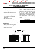
Sample & Buy Product Folder Support & Community Tools & Software Technical Documents TPS72710, TPS72711, TPS72715, TPS727185, TPS72718, TPS72719, TPS72725 TPS72727, TPS727285, TPS72728, TPS72730, TPS72733, TPS72748, TPS72750 SBVS128D – JUNE 2009 – REVISED FEBRUARY 2014 TPS727xx 250-mA, Ultralow IQ, Fast Transient Response, RF Low-Dropout Linear Regulator 1 Features 3 Description • The TPS727xx family of low-dropout (LDO) linear regulators are ultralow quiescent current LDOs with excellent line and
TPS72710, TPS72711, TPS72715, TPS727185, TPS72718, TPS72719, TPS72725 TPS72727, TPS727285, TPS72728, TPS72730, TPS72733, TPS72748, TPS72750 SBVS128D – JUNE 2009 – REVISED FEBRUARY 2014 www.ti.com Table of Contents 1 2 3 4 5 6 7 Features .................................................................. Applications ........................................................... Description ............................................................. Revision History.........................................
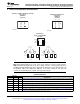
TPS72710, TPS72711, TPS72715, TPS727185, TPS72718, TPS72719, TPS72725 TPS72727, TPS727285, TPS72728, TPS72730, TPS72733, TPS72748, TPS72750 www.ti.com SBVS128D – JUNE 2009 – REVISED FEBRUARY 2014 5 Terminal Configuration and Functions TPS72715, TPS72718, TPS72728, TPS72748 YFF Package DSBGA-4 (Top View) OUT GND B2 B1 A2 IN All Other TPS727xx Devices YFF Package DSBGA-4 (Top View) OUT GND B2 B1 A2 A1 IN EN A1 EN See note. See note.
TPS72710, TPS72711, TPS72715, TPS727185, TPS72718, TPS72719, TPS72725 TPS72727, TPS727285, TPS72728, TPS72730, TPS72733, TPS72748, TPS72750 SBVS128D – JUNE 2009 – REVISED FEBRUARY 2014 www.ti.com 6 Specifications 6.1 Absolute Maximum Ratings (1) At TJ = –40°C to +125°C (unless otherwise noted). All voltages are with respect to GND. PARAMETER Input voltage range, VIN Enable voltage range, VEN TPS727xx UNIT –0.3 to +6.0 V –0.3 to +6.
TPS72710, TPS72711, TPS72715, TPS727185, TPS72718, TPS72719, TPS72725 TPS72727, TPS727285, TPS72728, TPS72730, TPS72733, TPS72748, TPS72750 www.ti.com SBVS128D – JUNE 2009 – REVISED FEBRUARY 2014 6.5 Electrical Characteristics Over operating temperature range (TJ = –40°C to +125°C), VIN = VOUT(TYP) + 0.3V or 2.0V, whichever is greater; IOUT = 10mA, VEN = 0.9V, and COUT = 1.0μF (unless otherwise noted). Typical values are at TJ = +25°C.
TPS72710, TPS72711, TPS72715, TPS727185, TPS72718, TPS72719, TPS72725 TPS72727, TPS727285, TPS72728, TPS72730, TPS72733, TPS72748, TPS72750 SBVS128D – JUNE 2009 – REVISED FEBRUARY 2014 www.ti.com 6.6 Typical Characteristics 1.90 1.90 1.88 1.88 1.86 1.86 1.84 1.84 1.82 1.82 VOUT (V) VOUT (V) Over operating temperature range (TJ = –40°C to +125°C), VIN = VOUT(TYP) + 0.3 V or 2.0 V, whichever is greater; IOUT = 10 mA, VEN = VIN, and COUT = 1.0 μF (unless otherwise noted).
TPS72710, TPS72711, TPS72715, TPS727185, TPS72718, TPS72719, TPS72725 TPS72727, TPS727285, TPS72728, TPS72730, TPS72733, TPS72748, TPS72750 www.ti.com SBVS128D – JUNE 2009 – REVISED FEBRUARY 2014 Typical Characteristics (continued) 1.90 12.0 1.88 11.5 1.86 11.0 1.84 10.5 IOUT = 10 mA 1.82 IGND (mA) VOUT (V) Over operating temperature range (TJ = –40°C to +125°C), VIN = VOUT(TYP) + 0.3 V or 2.0 V, whichever is greater; IOUT = 10 mA, VEN = VIN, and COUT = 1.0 μF (unless otherwise noted).
TPS72710, TPS72711, TPS72715, TPS727185, TPS72718, TPS72719, TPS72725 TPS72727, TPS727285, TPS72728, TPS72730, TPS72733, TPS72748, TPS72750 SBVS128D – JUNE 2009 – REVISED FEBRUARY 2014 www.ti.com Typical Characteristics (continued) Over operating temperature range (TJ = –40°C to +125°C), VIN = VOUT(TYP) + 0.3 V or 2.0 V, whichever is greater; IOUT = 10 mA, VEN = VIN, and COUT = 1.0 μF (unless otherwise noted). Typical values are at TJ = +25°C.
TPS72710, TPS72711, TPS72715, TPS727185, TPS72718, TPS72719, TPS72725 TPS72727, TPS727285, TPS72728, TPS72730, TPS72733, TPS72748, TPS72750 www.ti.com SBVS128D – JUNE 2009 – REVISED FEBRUARY 2014 Typical Characteristics (continued) Over operating temperature range (TJ = –40°C to +125°C), VIN = VOUT(TYP) + 0.3 V or 2.0 V, whichever is greater; IOUT = 10 mA, VEN = VIN, and COUT = 1.0 μF (unless otherwise noted). Typical values are at TJ = +25°C. 2 mV/div IOUT 10 mA 50 mV/div VOUT VOUT 2.7 V VIN 0.
TPS72710, TPS72711, TPS72715, TPS727185, TPS72718, TPS72719, TPS72725 TPS72727, TPS727285, TPS72728, TPS72730, TPS72733, TPS72748, TPS72750 SBVS128D – JUNE 2009 – REVISED FEBRUARY 2014 www.ti.com 7 Detailed Description 7.1 Overview The TPS727xx family belongs to a family of new generation LDO regulators that consume extremely low quiescent current while simulatenously delivering excellent PSRR with very little headroom (VIN – VOUT differential voltage), and very good transient response.
TPS72710, TPS72711, TPS72715, TPS727185, TPS72718, TPS72719, TPS72725 TPS72727, TPS727285, TPS72728, TPS72730, TPS72733, TPS72748, TPS72750 www.ti.com SBVS128D – JUNE 2009 – REVISED FEBRUARY 2014 Feature Description (continued) The TPS727xx automatically adjusts the soft-start current to supply both the load current and the COUT charge current. For example, if ILOAD = 0 mA upon enabling the LDO, ISOFT START = 1 μF × 0.07 V/μs + 0 mA = 70 mA, the current that charges the output capacitor.
TPS72710, TPS72711, TPS72715, TPS727185, TPS72718, TPS72719, TPS72725 TPS72727, TPS727285, TPS72728, TPS72730, TPS72733, TPS72748, TPS72750 SBVS128D – JUNE 2009 – REVISED FEBRUARY 2014 www.ti.com 8 Applications and Implementation 8.1 Application Information The TPS727xx family of low-dropout (LDO) linear regulators are utralow quiescent current LDOs with excellent line and ultra-fast load transient performance and are designed for power-sensitive applications. 8.2 Typical Application 8.2.1 TPS72718YFF 2.
TPS72710, TPS72711, TPS72715, TPS727185, TPS72718, TPS72719, TPS72725 TPS72727, TPS727285, TPS72728, TPS72730, TPS72733, TPS72748, TPS72750 www.ti.com SBVS128D – JUNE 2009 – REVISED FEBRUARY 2014 Typical Application (continued) Select adequate input and output capacitors. The startup current is given by Equation 2: ISOFT START (mA) = COUT(mF) ´ 0.07(V/ms) + ILOAD(mA) (2) This equation shows that soft-start current is directly proportional to COUT.
TPS72710, TPS72711, TPS72715, TPS727185, TPS72718, TPS72719, TPS72725 TPS72727, TPS727285, TPS72728, TPS72730, TPS72733, TPS72748, TPS72750 SBVS128D – JUNE 2009 – REVISED FEBRUARY 2014 www.ti.com Typical Application (continued) 2 mV/div IOUT 10 mA 50 mV/div VOUT VOUT 2.7 V VIN 0.5 V/div 100 mA/div 200 mA 2.1 V 1 ms/div 50 ms/div VIN = 2.3 V Slew Rate = 1 V/µs tR = tF = 1 µs IOUT = 100 µA Figure 32. Line Transient Response (TPS72718) Figure 31.
TPS72710, TPS72711, TPS72715, TPS727185, TPS72718, TPS72719, TPS72725 TPS72727, TPS727285, TPS72728, TPS72730, TPS72733, TPS72748, TPS72750 www.ti.com SBVS128D – JUNE 2009 – REVISED FEBRUARY 2014 8.3 Do's and Don'ts Do place at least one 1.0-µF ceramic capacitor as close as possible to the OUT terminal of the regulator. Do not place the output capacitor more than 10 mm away from the regulator. For DSE devices, do tie the NC terminals to ground to improve thermal dissipation. Do connect a 0.1-μF to 1.
TPS72710, TPS72711, TPS72715, TPS727185, TPS72718, TPS72719, TPS72725 TPS72727, TPS727285, TPS72728, TPS72730, TPS72733, TPS72748, TPS72750 SBVS128D – JUNE 2009 – REVISED FEBRUARY 2014 www.ti.com 10.2 Layout Example 10.2.1 DSE EVM Board Layout This section provides the TPS727xxDSEEVM-406 board layout and illustrations. Figure 37. Top Layer Assembly Figure 38.
TPS72710, TPS72711, TPS72715, TPS727185, TPS72718, TPS72719, TPS72725 TPS72727, TPS727285, TPS72728, TPS72730, TPS72733, TPS72748, TPS72750 www.ti.com SBVS128D – JUNE 2009 – REVISED FEBRUARY 2014 Layout Example (continued) Figure 39. Bottom Layer Routing Figure 40.
TPS72710, TPS72711, TPS72715, TPS727185, TPS72718, TPS72719, TPS72725 TPS72727, TPS727285, TPS72728, TPS72730, TPS72733, TPS72748, TPS72750 SBVS128D – JUNE 2009 – REVISED FEBRUARY 2014 www.ti.com Layout Example (continued) 10.2.2 YFF EVM Board Layout This section provides the TPS727xxYFFEVM-407 board layout and illustrations. Figure 41. Top Layer Assembly Figure 42.
TPS72710, TPS72711, TPS72715, TPS727185, TPS72718, TPS72719, TPS72725 TPS72727, TPS727285, TPS72728, TPS72730, TPS72733, TPS72748, TPS72750 www.ti.com SBVS128D – JUNE 2009 – REVISED FEBRUARY 2014 Layout Example (continued) Figure 43. Bottom Layer Routing Figure 44.
TPS72710, TPS72711, TPS72715, TPS727185, TPS72718, TPS72719, TPS72725 TPS72727, TPS727285, TPS72728, TPS72730, TPS72733, TPS72748, TPS72750 SBVS128D – JUNE 2009 – REVISED FEBRUARY 2014 www.ti.com 11 Device and Documentation Support 11.1 Related Links The table below lists quick access links. Categories include technical documents, support and community resources, tools and software, and quick access to sample or buy. Table 1.
TPS72710, TPS72711, TPS72715, TPS727185, TPS72718, TPS72719, TPS72725 TPS72727, TPS727285, TPS72728, TPS72730, TPS72733, TPS72748, TPS72750 www.ti.com SBVS128D – JUNE 2009 – REVISED FEBRUARY 2014 11.3 Trademarks Bluetooth is a registered trademark of Bluetooth SIG. Zigbee is a registered trademark of Zigbee Alliance. All other trademarks are the property of their respective owners. 11.4 Electrostatic Discharge Caution These devices have limited built-in ESD protection.
PACKAGE OUTLINE TPS727xxYFF YFF0004 DSBGA - 0.625 mm max height SCALE 13.000 DIE SIZE BALL GRID ARRAY B A E BALL A1 CORNER D 0.625 MAX C SEATING PLANE 0.30 0.12 BALL TYP 0.4 TYP B SYMM 0.4 TYP D: Max = 0.82 mm, Min = 0.76 mm E: Max = 1.19 mm, Min = 1.13 mm A 4X 0.015 C A 0.3 0.2 1 SYMM 2 B 02/2014 NanoFree Is a trademark of Texas Instruments. NOTES: 1. All linear dimensions are in millimeters. Any dimensions in parenthesis are for reference only.
EXAMPLE BOARD LAYOUT TPS727xxYFF YFF0004 DSBGA - 0.625 mm max height DIE SIZE BALL GRID ARRAY (0.4) TYP 4X 0.23 0.02 2 1 A SYMM (0.4) TYP B SYMM LAND PATTERN EXAMPLE SCALE:50X 0.05 MAX ( 0.23) METAL METAL UNDER MASK 0.05 MIN ( 0.23) SOLDER MASK OPENING SOLDER MASK OPENING NON-SOLDER MASK DEFINED (PREFERRED) SOLDER MASK DEFINED SOLDER MASK DETAILS NOT TO SCALE 02/2014 NOTES: (continued) 4.
EXAMPLE STENCIL DESIGN TPS727xxYFF YFF0004 DSBGA - 0.625 mm max height DIE SIZE BALL GRID ARRAY (0.4) TYP 4X ( 0.25) (R0.05) TYP 1 2 A SYMM (0.4) TYP B METAL TYP SYMM SOLDER PASTE EXAMPLE BASED ON 0.1 mm THICK STENCIL SCALE:50X 02/2014 NOTES: (continued) 5. Laser cutting apertures with trapezoidal walls and rounded corners may offer better paste release. www.ti.
PACKAGE OPTION ADDENDUM www.ti.
PACKAGE OPTION ADDENDUM www.ti.
PACKAGE OPTION ADDENDUM www.ti.
PACKAGE OPTION ADDENDUM www.ti.com 23-Jun-2014 (6) Lead/Ball Finish - Orderable Devices may have multiple material finish options. Finish options are separated by a vertical ruled line. Lead/Ball Finish values may wrap to two lines if the finish value exceeds the maximum column width. Important Information and Disclaimer:The information provided on this page represents TI's knowledge and belief as of the date that it is provided.
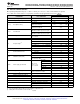
PACKAGE MATERIALS INFORMATION www.ti.com 13-Mar-2014 TAPE AND REEL INFORMATION *All dimensions are nominal Device Package Package Pins Type Drawing SPQ Reel Reel A0 Diameter Width (mm) (mm) W1 (mm) B0 (mm) K0 (mm) P1 (mm) W Pin1 (mm) Quadrant TPS72710DSER WSON DSE 6 3000 179.0 8.4 1.8 1.8 1.0 4.0 8.0 Q2 TPS72710DSER WSON DSE 6 3000 180.0 8.4 1.7 1.7 0.95 4.0 8.0 Q2 TPS72710DSET WSON DSE 6 250 179.0 8.4 1.8 1.8 1.0 4.0 8.
PACKAGE MATERIALS INFORMATION www.ti.com 13-Mar-2014 Device Package Package Pins Type Drawing SPQ Reel Reel A0 Diameter Width (mm) (mm) W1 (mm) B0 (mm) K0 (mm) P1 (mm) W Pin1 (mm) Quadrant TPS72719DSET WSON DSE 6 250 179.0 8.4 1.8 1.8 1.0 4.0 8.0 Q2 TPS72719DSET WSON DSE 6 250 180.0 8.4 1.7 1.7 0.95 4.0 8.0 Q2 TPS72719YFFR DSBGA YFF 4 3000 180.0 8.4 0.89 1.26 0.69 4.0 8.0 Q1 TPS72719YFFT DSBGA YFF 4 250 180.0 8.4 0.89 1.26 0.69 4.0 8.
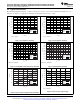
PACKAGE MATERIALS INFORMATION www.ti.com 13-Mar-2014 *All dimensions are nominal Device Package Type Package Drawing Pins SPQ Length (mm) Width (mm) Height (mm) TPS72710DSER WSON DSE 6 3000 203.0 203.0 35.0 TPS72710DSER WSON DSE 6 3000 205.0 200.0 33.0 TPS72710DSET WSON DSE 6 250 203.0 203.0 35.0 TPS72710DSET WSON DSE 6 250 205.0 200.0 33.0 TPS72711YFFR DSBGA YFF 4 3000 182.0 182.0 17.0 TPS72711YFFT DSBGA YFF 4 250 182.0 182.0 17.
PACKAGE MATERIALS INFORMATION www.ti.com 13-Mar-2014 Device Package Type Package Drawing Pins SPQ Length (mm) Width (mm) Height (mm) TPS72719YFFR DSBGA YFF 4 3000 182.0 182.0 17.0 TPS72719YFFT DSBGA YFF 4 250 182.0 182.0 17.0 TPS72725DSER WSON DSE 6 3000 203.0 203.0 35.0 TPS72725DSET WSON DSE 6 250 203.0 203.0 35.0 TPS72727DSER WSON DSE 6 3000 205.0 200.0 33.0 TPS72727DSER WSON DSE 6 3000 203.0 203.0 35.0 TPS72727DSET WSON DSE 6 250 205.0 200.
IMPORTANT NOTICE Texas Instruments Incorporated and its subsidiaries (TI) reserve the right to make corrections, enhancements, improvements and other changes to its semiconductor products and services per JESD46, latest issue, and to discontinue any product or service per JESD48, latest issue. Buyers should obtain the latest relevant information before placing orders and should verify that such information is current and complete.