
Datasheet

3
2
4
5
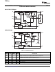
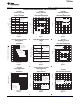
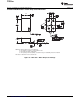
DBV PACKAGE
(TOP VIEW)
1IN
GND
EN
OUT
NR
Fixed Option
3
2
4
6
DBV PACKAGE
(TOP VIEW)
1
IN
GND
EN
OUT
NR
5
FB
Adjustable Option
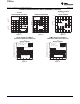
TPS73028
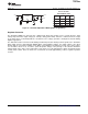
RIPPLE REJECTION
vs
FREQUENCY
10 100 1 k 10 k
10
40
80
100 k 1 M 10 M
Ripple Rejection (dB)
Frequency (Hz)
I
OUT
= 10 mA
50
0
V
IN
= 3.8 V
C
OUT
= 10 µF
C
NR
= 0.01 µF
I
OUT
= 200 mA
20
30
60
70
90
100
0
0.05
0.10
0.15
0.20
0.25
0.30
100 1 k 10 k 100 k
Frequency (Hz)
I
OUT
= 1 mA
V
IN
= 3.8 V
C
OUT
= 2.2 µF
C
NR
= 0.1 µF
I
OUT
= 200 mA
TPS73028
OUTPUT SPECTRAL NOISE DENSITY
vs
FREQUENCY
Output Spectral Noise Density (µV/√Hz)
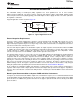
IN
EN
OUT
NR
GND
YZQ PACKAGE
(TOP VIEW)
A3 A1
C3 C1
B2
TPS730xx
www.ti.com
SBVS054I – NOVEMBER 2004– REVISED FEBRUARY 2011
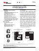
LOW-NOISE, HIGH PSRR, RF 200-mA
LOW-DROPOUT LINEAR REGULATORS
Check for Samples: TPS730xx
1
FEATURES
DESCRIPTION
234
• 200-mA RF Low-Dropout Regulator
The TPS730xx family of low-dropout (LDO)
With Enable
low-power linear voltage regulators features high
power-supply rejection ratio (PSRR), ultralow-noise,
• Available in Fixed Voltages from 1.8V to 3.3V
fast start-up, and excellent line and load transient
and Adjustable (1.22V to 5.5V)
responses a small SOT23 package. NanoStar™
• High PSRR (68dB at 100Hz)
packaging gives an ultrasmall footprint as well as an
• Ultralow-Noise (33μV
RMS
, TPS73018)
ultralow profile and package weight, making it ideal
for portable applications such as handsets and PDAs.
• Fast Start-Up Time (50μs)
Each device in the family is stable, with a small 2.2μF
• Stable With a 2.2μF Ceramic Capacitor
ceramic capacitor on the output. The TPS730xx
• Excellent Load/Line Transient Response
family uses an advanced, proprietary BiCMOS
fabrication process to yield low dropout voltages (e.g.,
• Very Low Dropout Voltage (120mV at 200mA)
120mV at 200mA, TPS73030). Each device achieves
• 5- and 6-Pin SOT23 (DBV), and Wafer Chip
fast start-up times (approximately 50μs with a
Scale (YZQ) Packages
0.001μF bypass capacitor) while consuming low
quiescent current (170μA typical). Moreover, when
APPLICATIONS
the device is placed in standby mode, the supply
• RF: VCOs, Receivers, ADCs
current is reduced to less than 1μA. The TPS73018
exhibits approximately 33μV
RMS
of output voltage
• Audio
noise at 1.8V output with a 0.01μF bypass capacitor.
• Cellular and Cordless Telephones
Applications with analog components that are
• Bluetooth
®
, Wireless LAN
noise-sensitive, such as portable RF electronics,
• Handheld Organizers, PDAs
benefit from the high PSRR and low-noise features
as well as the fast response time.
Figure 1.
1
Please be aware that an important notice concerning availability, standard warranty, and use in critical applications of Texas
Instruments semiconductor products and disclaimers thereto appears at the end of this data sheet.
2NanoStar is a trademark of Texas Instruments.
3Bluetooth is a registered trademark of Bluetooth Sig, Inc.
4All other trademarks are the property of their respective owners.
PRODUCTION DATA information is current as of publication date.
© 2004–2011, Texas Instruments Incorporated
Products conform to specifications per the terms of the Texas
Instruments standard warranty. Production processing does not
necessarily include testing of all parameters.