
Datasheet
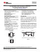

IN
N/C
N/C
EN
8
7
6
5
OUT
N/C
NR/FB
GND
1
2
3
4
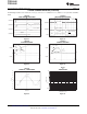
TPS732xx
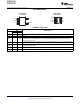
GNDEN NR
IN OUT
V
IN
V
OUT
Optional
Optional Optional
Typical Application Circuit for Fixed-Voltage Versions
IN
GND
EN 3 NR/FB
OUT1
2
5
4
TPS73201-Q1
TPS73225-Q1
www.ti.com
SGLS303E –MAY 2005–REVISED AUGUST 2013
CAP-FREE NMOS 250-mA LOW-DROPOUT REGULATOR
WITH REVERSE-CURRENT PROTECTION
Check for Samples: TPS73201-Q1, TPS73225-Q1
1
FEATURES
APPLICATIONS
• Qualified for Automotive Applications • Portable/Battery-Powered Equipment
• Stable with No Output Capacitor or Any Value • Post-Regulation for Switching Supplies
or Type of Capacitor
• Noise-Sensitive Circuitry Such as VCOs
• Input Voltage Range: 1.7 V to 5.5 V
• Point of Load Regulation for DSPs, FPGAs,
• Ultralow Dropout Voltage: ASICs, and Microprocessors
40 mV Typ at 250 mA
DESCRIPTION
• Excellent Load Transient Response—With or
The TPS732xx family of low-dropout (LDO) voltage
Without Optional Output Capacitor
regulators uses a new topology: an NMOS pass
• New NMOS Topology Provides Low Reverse
element in a voltage-follower configuration. This
Leakage Current
topology is stable using output capacitors with low
• Low Noise: 30 μV
RMS
Typ (10 kHz to 100 kHz)
ESR, and even allows operation without a capacitor.
It also provides high reverse blockage (low reverse
• 0.5% Initial Accuracy
current) and ground pin current that is nearly constant
• 1% Overall Accuracy (Line, Load, and
over all values of output current.
Temperature)
The TPS732xx uses an advanced BiCMOS process
• Less Than 1 μA Max I
Q
in Shutdown Mode
to yield high precision while delivering low dropout
• Thermal Shutdown and Specified Min/Max
voltages and low ground pin current. Current
Current Limit Protection
consumption, when not enabled, is under 1 μA and
• Available in Multiple Output Voltage Versions
ideal for portable applications. The extremely low
output noise (30 μV
RMS
with 0.1 µF C
NR
) is ideal for
– Fixed Outputs of 1.2 V, 1.5 V, 1.6 V, 1.8 V,
powering VCOs. These devices are protected by
2.5 V, 3 V, 3.3 V, and 5 V
thermal shutdown and foldback current limit.
– Adjustable Outputs From 1.2 V to 5.5 V
– Custom Outputs Available
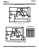
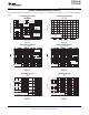
DBV PACKAGE
(TOP VIEW)
DRB PACKAGE
(TOP VIEW)
Figure 1.
1
Please be aware that an important notice concerning availability, standard warranty, and use in critical applications of
Texas Instruments semiconductor products and disclaimers thereto appears at the end of this data sheet.
UNLESS OTHERWISE NOTED this document contains
Copyright © 2005–2013, Texas Instruments Incorporated
PRODUCTION DATA information current as of publication date.
Products conform to specifications per the terms of Texas
Instruments standard warranty. Production processing does not
necessarily include testing of all parameters.