
Datasheet

1
FEATURES
APPLICATIONS
DESCRIPTION/ORDERING INFORMATION
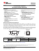
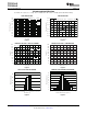
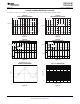
Typical Application Circuit
TPS737xx
GNDEN
FB
IN OUT
V
IN
V
OUT
Optional
1.0 µF
OFF
ON
IN
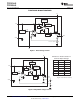
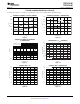
NC
NC
EN
8
7
6
5
OUT
NC
NR/FB
GND
1
2
3
4
DRB PACKAGE
(TOP VIEW)
NC – No internal connection
TPS73719-Q1
TPS73733-Q1
www.ti.com
........................................................................................................................................................................................... SBVS123 – DECEMBER 2008
1-A LOW-DROPOUT REGULATOR
WITH REVERSE CURRENT PROTECTION
2
• Qualified for Automotive Applications • Thermal Shutdown and Current Limit for Fault
Protection
• Stable with 1.0- µ F or Larger Ceramic Output
Capacitor • Available in Multiple Output Voltage Versions
• Input Voltage Range: 2.2 V to 5.5 V – Adjustable Output: 1.20 V to 5.5 V
• Ultra-Low Dropout Voltage: 130 mV typ at 1 A – Custom Outputs Available Using Factory
Package-Level Programming
• Excellent Load Transient Response, Even With
Only 1.0- µ F Output Capacitor
• NMOS Topology Delivers Low Reverse
• Point of Load Regulation for DSPs, FPGAs,
Leakage Current
ASICs, and Microprocessors
• 1.0% Initial Accuracy
• Post-Regulation for Switching Supplies
• 3% Overall Accuracy Over Line, Load, and
• Portable/Battery-Powered Equipment
Temperature
• Less Than 20-nA (Typ) Quiescent Current in
Shutdown Mode
The TPS737xx family of linear low-dropout (LDO) voltage regulators uses an NMOS pass element in a
voltage-follower configuration. This topology is relatively insensitive to output capacitor value and ESR, allowing
a wide variety of load configurations. Load transient response is excellent, even with a small 1.0- µ F ceramic
output capacitor. The NMOS topology also allows very low dropout.
The TPS737xx family uses an advanced BiCMOS process to yield high precision while delivering very low
dropout voltages and low ground pin current. Current consumption, when not enabled, is under 20 nA and ideal
for portable applications. These devices are protected by thermal shutdown and foldback current limit.
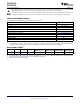
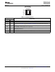
ORDERING INFORMATION
(1)
T
A
V
OUT
(TYP) PACKAGE
(2)
ORDERABLE PART NUMBER TOP-SIDE MARKING
3.3 V TPS73733QDRBRQ1 733Q
– 40 ° C to 125 ° C 1.9 V SON – DRB Reel of 3000 TPS73719QDRBRQ1 719Q
Adjustable TPS73701QDRBRQ1 PREVIEW
(1) For the most current package and ordering information, see the Package Option Addendum at the end of this document, or see the TI
web site at www.ti.com .
(2) Package drawings, thermal data, and symbolization are available at www.ti.com/packaging .
1
Please be aware that an important notice concerning availability, standard warranty, and use in critical applications of Texas
Instruments semiconductor products and disclaimers thereto appears at the end of this data sheet.
2 All trademarks are the property of their respective owners.
UNLESS OTHERWISE NOTED this document contains
Copyright © 2008, Texas Instruments Incorporated
PRODUCTION DATA information current as of publication date.
Products conform to specifications per the terms of Texas
Instruments standard warranty. Production processing does not
necessarily include testing of all parameters.