
Datasheet

TPS74401
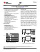
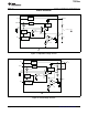
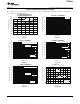
GND
EN
FB
IN PG
SS
OUT
V
IN
V
OUT
V
PG
R
1
R
2
R
3
C
OUT
Optional
C
IN
1 Fm
C
SS
V
BIAS
C
BIAS
1 Fm
BIAS
TPS744xx
GND
EN
SNS
IN PG
SS
OUT
V
IN
V
OUT
V
PG
R
3
C
OUT
Optional
C
IN
1 Fm
C
SS
V
BIAS
C
BIAS
1 Fm
BIAS
ADJUSTABLEVOLTAGEVERSION
FIXEDVOLTAGEVERSION
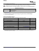
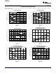
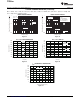
1V/div
500mV/div
Time(1ms/div)
C =0 F
SS
m
C =0.001 F
SS
m
C =0.0047 F
SS
m
V
OUT
V
EN
0V
1.1V
TPS744xx
TPS744xx
TPS744xx
www.ti.com
SBVS066O –DECEMBER 2005–REVISED MARCH 2013
3.0A Ultra-LDO with Programmable Soft-Start
Check for Samples: TPS744xx
1
FEATURES
DESCRIPTION
2
• Soft-Start (SS) Pin Provides a Linear Startup
The TPS744xx low-dropout (LDO) linear regulators
with Ramp Time Set by External Capacitor
provide an easy-to-use robust power management
• 1% Accuracy Over Line, Load, and
solution for a wide variety of applications. User-
Temperature
programmable soft-start minimizes stress on the input
power source by reducing capacitive inrush current
• Supports Input Voltages as Low as 0.9V with
on start-up. The soft-start is monotonic and well-
External Bias Supply
suited for powering many different types of
• Adjustable Output (0.8V to 3.6V)
processors and ASICs. The enable input and power-
• Fixed Output (0.9V to 3.6V)
good output allow easy sequencing with external
regulators. This complete flexibility permits the user to
• Ultra-Low Dropout: 115mV at 3.0A (typ)
configure a solution that will meet the sequencing
• Stable with Any or No Output Capacitor
requirements of FPGAs, DSPs, and other
• Excellent Transient Response
applications with specific start-up requirements.
• Available in 5mm × 5mm × 1mm QFN and
A precision reference and error amplifier deliver 1%
DDPAK-7 Packages
accuracy over load, line, temperature, and process.
Each LDO is stable with low-cost ceramic output
• Open-Drain Power-Good (QFN only)
capacitors and the device family is fully specified from
• Active High Enable
–40°C to +125°C. The TPS744xx is offered in a small
(5mm × 5mm) QFN package, yielding a highly
APPLICATIONS
compact total solution size. For applications that
• FPGA Applications require additional power dissipation, the DDPAK
(KTW) package is also available.
• DSP Core and I/O Voltages
space
• Post-Regulation Applications
• Applications with Special Start-Up Time or
Sequencing Requirements
• Hot-Swap and Inrush Controls
space
Figure 1. Turn-On Response
Figure 2. Typical Application Circuits
1
Please be aware that an important notice concerning availability, standard warranty, and use in critical applications of
Texas Instruments semiconductor products and disclaimers thereto appears at the end of this data sheet.
2All trademarks are the property of their respective owners.
PRODUCTION DATA information is current as of publication date.
Copyright © 2005–2013, Texas Instruments Incorporated
Products conform to specifications per the terms of the Texas
Instruments standard warranty. Production processing does not
necessarily include testing of all parameters.