TPS75105DSK Evaluation Module (EVM) User's Guide Literature Number: SLVU334 August 2009
SLVU334 – August 2009 Submit Documentation Feedback Copyright © 2009, Texas Instruments Incorporated
Preface SLVU334 – August 2009 About This Manual This User’s Guide describes the characteristics, operation, and use of the TPS75105DSKEVM-529 Evaluation Module (EVM). This EVM demonstrates the Texas Instruments TPS75105 low-dropout, two-bank LED driver with PWM brightness control. This User’s Guide includes setup instructions, a schematic diagram, a bill of materials (BOM), and PCB layout drawings for the evaluation module.
SLVU334 – August 2009 Submit Documentation Feedback Copyright © 2009, Texas Instruments Incorporated
Chapter 1 SLVU334 – August 2009 Introduction The Texas Instruments TPS75105DSKEVM-529 evaluation module (EVM) helps designers evaluate the operation and performance of the TPS75105 low-dropout linear regulator (LDO), two-bank LED driver with PWM dimming. The TPS75105 contains four current-regulated LED driver outputs and operates from a 2.7-V to 5.5-V input supply. The IC drives the anodes of two banks of two LEDs. Each bank is independently enabled and can be dimmed using a PWM signal to the EN pin.
Introduction SLVU334 – August 2009 Submit Documentation Feedback Copyright © 2009, Texas Instruments Incorporated
Chapter 2 SLVU334 – August 2009 Setup This chapter describes the jumpers and connectors on the EVM, as well as how to properly connect, set up, and use the TPS75105DSKEVM-529. 2.1 Input / Output Connector Descriptions J1 – VIN This is the positive input-voltage connection to the converter. The EVM operates from any supply voltage between 2.7 V and 5.5 V. The leads to the input supply should be twisted and kept as short as possible to minimize EMI transmission and input voltage droop.
Setup www.ti.com JP6 – LED D2B Cathode Connection JP6 is used to measure the current through LED D2B. Place a current meter between the pins of JP6 to measure the current. Alternatively, a resistor may be connected between the pins of JP6 in order to measure the current as a voltage. Place a shorting bar across the pins of JP6 if current measurement is not required. PCB pads are provided to install a current-sense resistor across this jumper. 2.2 Setup 2.2.
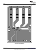
Chapter 3 SLVU334 – August 2009 Board Layout This chapter provides the TPS75105DSKEVM-529 board layout and illustrations. 3.1 Layout Figure 3-1, Figure 3-2, and Figure 3-3 show the board layout for the TPS75105DSKEVM-529 PWB. Figure 3-1.
Layout www.ti.com Figure 3-2.
Layout www.ti.com Figure 3-3.
Board Layout SLVU334 – August 2009 Submit Documentation Feedback Copyright © 2009, Texas Instruments Incorporated
Chapter 4 SLVU334 – August 2009 Schematic and Bill of Materials This chapter provides the TPS75105DSKEVM-529 schematic and bill of materials. 4.1 Schematic The TSP75105DSK may operate at temperatures above 85°C. S001 Figure 4-1.
Bill of Materials 4.2 www.ti.com Bill of Materials Table 4-1 is the bill of materials for the TPS75105DSKEVM-529 EVM. Table 4-1. Bill of Materials Count RefDes Value 1 C1 1 µF 4 D1A1, SML-LX2832UWC-TR D1B1, D2A1, D2B1 2 J1, J2 2 Description Capacitor, ceramic, 16-V, X5R, 10% Size 0603 Part Number MFR STD STD Diode, LED, white, 30-mA 1210 SML-LX2832UWC-TR Lumex PEC02SAAN Header, 2-pin, 100-mil spacing 0.1 inch (2.
Bill of Materials www.ti.com EVM WARNINGS AND RESTRICTIONS It is important to operate this EVM within the input voltage range of 2.7 V to 5.5 V and the output current range of 3 mA to 25 mA through each LED. Exceeding the specified input range may cause unexpected operation and/or irreversible damage to the EVM. If there are questions concerning the input range, please contact a TI field representative prior to connecting the input power.