
Datasheet

SGLS247A − JUNE 2004 − REVISED JUNE 2008
www.ti.com
D Qualified for Automotive Applications
D 150-mA Low-Dropout Regulator
D Output Voltage: 5 V, 3.8 V, 3.3 V, 3 V, 2.8 V,
2.7 V, 2.5 V, 1.8 V, 1.6 V and Variable
D Dropout Voltage, Typically 300 mV
at 150 mA
D Thermal Protection
D Overcurrent Limitation
D Less Than 2-µA Quiescent Current in
Shutdown Mode
D −40°C to 125°C Operating Junction
Temperature Range
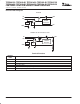
D 5-Pin SOT-23 (DBV) Package
description
The TPS763xx family of low-dropout (LDO) voltage regulators offers the benefits of low-dropout voltage, low-power
operation, and miniaturized packaging. These regulators feature low dropout voltages and quiescent currents compared
to conventional LDO regulators. Offered in a 5-terminal, small outline integrated-circuit SOT-23 package, the TPS763xx
series devices are ideal for cost-sensitive designs and for applications where board space is at a premium.
A combination of new circuit design and process innovation has enabled the usual pnp pass transistor to be replaced by
a PMOS pass element. Because the PMOS pass element behaves as a low-value resistor, the dropout voltage is
low—typically 300 mV at 150 mA of load current (TPS76333)—and is directly proportional to the load current. Since the
PMOS pass element is a voltage-driven device, the quiescent current is low (140 µA maximum) and is stable over the entire
range of output load current (0 mA to 150 mA). Intended for use in portable systems such as laptops and cellular phones,
the low-dropout voltage feature and low-power operation result in a significant increase in system battery operating life.
The TPS763xx also features a logic-enabled sleep mode to shut down the regulator, reducing quiescent current to 1 µA
maximum at T
J
= 25°C.The TPS763xx is offered in 1.6-V,1.8-V, 2.5-V, 2.7-V, 2.8-V, 3-V, 3.3-V, 3.8-V, and 5-V fixed-voltage
versions and in a variable version (programmable over the range of 1.5 V to 6.5 V).
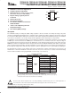
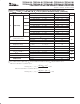
AVAILABLE OPTIONS
{
T
J
VOLTAGE PACKAGE
}
PART NUMBER SYMBOL
Variable TPS76301QDBVRQ1 BAN
1.6 V TPS76316QDBVRQ1 BAD
1.8 V TPS76318QDBVRQ1 BAP
2.5 V TPS76325QDBVRQ1 BAQ
−40°C to 125°C
2.7 V
SOT-23
TPS76327QDBVRQ1
§
−40°C to 125°C
2.8 V
SOT-23
(DBV)
TPS76328QDBVRQ1
§
3 V
(DBV)
TPS76330QDBVRQ1 BAT
3.3 V TPS76333QDBVRQ1 BAU
3.8 V TPS76338QDBVRQ1
§
5.0 V TPS76350QDBVRQ1 BAW
†
For the most current package and ordering information, see the Package Option Addendum at
the end of this document, or see the TI web site at http://www.ti.com.
‡
Package drawings, thermal data, and symbolization are available at http://www.ti.com/packaging.
§
Product Preview. Contact Texas Instruments for availability.
Copyright 2008 Texas Instruments Incorporated
!"# $ %&!!'# "$ (&)*%"# +"#', !+&%#$
%! # $('%%"#$ ('! #-' #'!$ '."$ $#!&'#$ $#"+"!+ /"!!"#0,
!+&%# (!%'$$1 +'$ # '%'$$"!*0 %*&+' #'$#1 "** ("!"'#'!$,
Please be aware that an important notice concerning availability, standard warranty, and use in critical applications of
Texas Instruments semiconductor products and disclaimers thereto appears at the end of this data sheet.
All trademarks are the property of their respective owners.
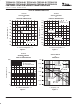
3
2
4
5
DBV PACKAGE
(TOP VIEW)
1
IN
GND
EN
OUT
NC/FB