
Datasheet

1
FEATURES
DESCRIPTION
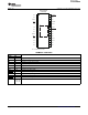
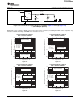
NC
NC
1GND
1IN
1IN
NC
NC
2GND
2IN
2IN
NC
NC
NC=Nointernalconnection
NC
NC
1FB/NC
1OUT
1OUT
NC
NC
NC
2OUT
2OUT
NC
NC
1
2
3
4
5
6
7
8
9
10
11
12
13
14
28
27
26
25
24
23
22
21
20
19
18
17
16
15
1EN
2EN
2RESET
1RESET
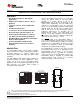
PWPPACKAGE
(TOPVIEW)
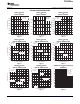
0 20 20040 60 80 100 120 140 160 180
LINETRANSIENTRESPONSE
V =3.3V
C =10 F
T =25 C
OUT
L
A
m
°
5.3
4.3
10
0
-10
t Time s- - m
D -
-
V Changein
OutputV
oltage mV
O
UT
V
InputVoltage V
IN
- -
V
DropoutVoltage mV
D
O
- -
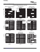
10
3
10
2
10
1
10
-1
10
-2
10
-60 -40 -20 0 20 40 60 80 100 120 140
T Free-AirTemperature C
A
- - °
V =3.3V
C =10 F
OUT
OUT
m
I =0
OUT
I =10mA
OUT
I =1A
OUT
DROPOUTVOLTAGE
vsFREE-AIRTEMPERATURE
TPS767D3xx
www.ti.com
......................................................................................................................................................... SLVS209H – JULY 1999 – REVISED AUGUST 2008
DUAL-OUTPUT LOW-DROPOUT VOLTAGE REGULATORS
Because the PMOS device behaves as a low-value
23
• Dual Output Voltages for Split-Supply
resistor, the dropout voltage is very low (350mV
Applications
typically at an output current of 1A for the
• Output Current Range of 0mA to 1.0A per
TPS767D325) and is directly proportional to the
Regulator
output current. Additionally, since the PMOS pass
• 3.3V/2.5V, 3.3V/1.8V, and 3.3V/Adjustable
element is a voltage-driven device, the quiescent
Output
current is very low and independent of output loading
(typically 85 µ A over the full range of output current,
• Fast-Transient Response
0mA to 1A). These two key specifications yield a
• 2% Tolerance Over Load and Temperature
significant improvement in operating life for
• Dropout Voltage Typically 350mV at 1A
battery-powered systems. This LDO family also
features a sleep mode; applying a TTL high signal to
• Ultra-low 85 µ A Typical Quiescent Current
EN (enable) shuts down the regulator, reducing the
• 1 µ A Quiescent Current During Shutdown
quiescent current to 1 µ A at T
J
= +25 ° C.
• Dual Open-Drain Power-On Reset with 200ms
The RESET output of the TPS767D3xx initiates a
Delay for Each Regulator
reset in microcomputer and microprocessor systems
• 28-Pin PowerPAD™ TSSOP Package
in the event of an undervoltage condition. An internal
• Thermal Shutdown Protection for Each comparator in the TPS767D3xx monitors the output
voltage of the regulator to detect an undervoltage
Regulator
condition on the regulated output voltage.
The TPS767D3xx is offered in 1.8V, 2.5V, and 3.3V
fixed-voltage versions and in an adjustable version
The TPS767D3xx family of dual voltage regulators
(programmable over the range of 1.5V to 5.5V).
offers fast transient response, low dropout voltages
Output voltage tolerance is specified as a maximum
and dual outputs in a compact package and
of 2% over line, load, and temperature ranges. The
incorporating stability with 10 µ F low ESR output
TPS767D3xx family is available in a 28-pin PWP
capacitors.
TSSOP package. They operate over a junction
The TPS767D3xx family of dual voltage regulators is
temperature range of – 40 ° C to +125 ° C.
designed primarily for DSP applications. These
devices can be used in any mixed-output voltage
application, with each regulator supporting up to 1A.
Dual active-low reset signals allow resetting of
core-logic and I/O separately.
1
Please be aware that an important notice concerning availability, standard warranty, and use in critical applications of Texas
Instruments semiconductor products and disclaimers thereto appears at the end of this data sheet.
2 PowerPAD is a trademark of Texas Instruments.
3 All other trademarks are the property of their respective owners.
PRODUCTION DATA information is current as of publication date.
Copyright © 1999 – 2008, Texas Instruments Incorporated
Products conform to specifications per the terms of the Texas
Instruments standard warranty. Production processing does not
necessarily include testing of all parameters.