
Datasheet

TPS76815-Q1, TPS76818-Q1, TPS76825-Q1, TPS76827-Q1
TPS76828-Q1, TPS76830-Q1 TPS76833-Q1, TPS76850-Q1, TPS76801-Q1
FAST-TRANSIENT-RESPONSE 1-A LOW-DROPOUT VOLTAGE REGULATORS
SGLS155A − FEBRUARY 2003 − REVISED SEPTEMBER 2008
1
POST OFFICE BOX 655303 • DALLAS, TEXAS 75265
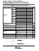
D Qualified for Automotive Applications
D ESD Protection Exceeds 2000 V Per
MIL-STD-883, Method 3015; Exceeds 200 V
Using Machine Model (C = 200 pF, R = 0)
D 1-A Low-Dropout Voltage Regulator
D Available in 1.5-V, 1.8-V, 2.5-V, 2.7-V, 2.8-V,
3.0-V, 3.3-V, 5.0-V Fixed Output and
Adjustable Versions
D Dropout Voltage Down to 230 mV at 1 A
(TPS76850)
D Ultralow 85-µA Typical Quiescent Current
D Fast Transient Response
D 2% Tolerance Over Specified Conditions for
Fixed-Output Versions
D Open-Drain Power Good (See TPS767xx for
Power-On Reset With 200-ms Delay Option)
D 20-Pin TSSOP (PWP) Package
D Thermal Shutdown Protection
description
This device is designed to have a fast transient response and be stable with 10-µF low ESR capacitors. This
combination provides high performance at a reasonable cost.
Because the PMOS device behaves as a low-value resistor, the dropout voltage is very low (typically 230 mV
at an output current of 1 A for the TPS76850) and is directly proportional to the output current. Additionally, since
the PMOS pass element is a voltage-driven device, the quiescent current is very low and independent of output
loading (typically 85 µA over the full range of output current, 0 mA to 1 A). These two key specifications yield
a significant improvement in operating life for battery-powered systems. This LDO family also features a sleep
mode; applying a TTL high signal to EN
(enable) shuts down the regulator, reducing the quiescent current to
less than 1 µA at T
J
= 25°C.
Power good (PG) is an active high output, which can be used to implement a power-on reset or a low-battery
indicator.
The TPS768xx is offered in 1.5-V, 1.8-V, 2.5-V, 2.7-V, 2.8-V, 3.0-V, 3.3-V, and 5.0-V fixed-voltage versions and
in an adjustable version (programmable over the range of 1.2 V to 5.5 V). Output voltage tolerance is specified
as a maximum of 2% over line, load, and temperature ranges. The TPS768xx family is available in a 20-pin PWP
package.
Copyright 2008, Texas Instruments Incorporated
PRODUCTION DATA information is current as of publication date.
Products conform to specifications per the terms of Texas Instruments
standard warranty. Production processing does not necessarily include
testing of all parameters.
Please be aware that an important notice concerning availability, standard warranty, and use in critical applications of
Texas Instruments semiconductor products and disclaimers thereto appears at the end of this data sheet.
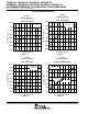
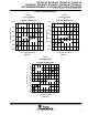
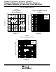
NC − No internal connection
1
2
3
4
5
6
7
8
9
10
20
19
18
17
16
15
14
13
12
11
GND/HSINK
GND/HSINK
GND
NC
EN
IN
IN
NC
GND/HSINK
GND/HSINK
GND/HSINK
GND/HSINK
NC
NC
PG
FB/NC
OUT
OUT
GND/HSINK
GND/HSINK
PWP PACKAGE
(TOP VIEW)