
Datasheet


www.ti.com
FEATURES DESCRIPTION
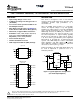
PG
OUT
OUT
7
6
5
IN
IN
EN
GND
3
16
14
13
V
I
0.1 µF
PG
V
O
10 µF
+
TPS768xx
C
o
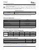
GND
EN
IN
IN
PG
FB/NC
OUT
OUT
1
2
3
4
8
7
6
5
D PACKAGE
(Top View)
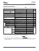
GND/HSINK
GND/HSINK
GND
NC
EN
IN
IN
NC
GND/HSINK
GND/HSINK
GND/HSINK
GND/HSINK
NC
NC
PG
FB/NC
OUT
OUT
GND/HSINK
GND/HSINK
1
2
3
4
5
6
7
8
9
10
20
19
18
17
16
15
14
13
12
11
PWP PACKAGE
(Top View)
NC = No Internal Connection
TPS768xxQ
SLVS211L – JUNE 1999 – REVISED JANUARY 2006
FAST TRANSIENT RESPONSE, 1-A LOW-DROPOUT VOLTAGE REGULATORS
• Input Voltage Range: 2.7 V to 10 V
This device is designed to have a fast transient
response and be stable with 10 µ F capacitors. This
• Low-Dropout Voltage: 230 mV typical at 1 A
combination provides high performance at a
(TPS76850)
reasonable cost.
• 2% Tolerance Over Specified Conditions for
Since the PMOS device behaves as a low-value
Fixed-Output Versions
resistor, the dropout voltage is very low (typically
• Open Drain Power Good (See TPS767xx for
230 mV at an output current of 1 A for the TPS76850)
Power-On Reset With 200-ms Delay Option)
and is directly proportional to the output current.
• Ultralow 85 µ A Typical Quiescent Current
Additionally, because the PMOS pass element is a
voltage-driven device, the quiescent current is very
• Available in 1.5-V, 1.8-V, 2.5-V, 2.7-V, 2.8-V,
low and independent of output loading (typically
3.0-V, 3.3-V, 5.0-V Fixed Output and
85 µ A over the full range of output current, 0 mA to
Adjustable (1.2 V to 5.5 V) Versions
1 A). These two key specifications yield a significant
• Fast Transient Response
improvement in operating life for battery-powered
• Thermal Shutdown Protection
systems. This LDO family also features a shutdown
mode; applying a TTL high signal to EN (enable)
• SOIC-8 (D) and TSSOP-20 (PWP) Package
shuts down the regulator, reducing the quiescent
current to less than 1 µ A at T
J
= 25 ° C.
Power good (PG) is an active high output, which can
be used to implement a power-on reset or a
low-battery indicator.
Figure 1. Typical Application Configuration
(For Fixed Output Options)
Please be aware that an important notice concerning availability, standard warranty, and use in critical applications of Texas
Instruments semiconductor products and disclaimers thereto appears at the end of this data sheet.
All trademarks are the property of their respective owners.
PRODUCTION DATA information is current as of publication date.
Copyright © 1999–2006, Texas Instruments Incorporated
Products conform to specifications per the terms of the Texas
Instruments standard warranty. Production processing does not
necessarily include testing of all parameters.