
Datasheet

TI Information — Selective Disclosure
TPS780 Series
SBVS083D –JANUARY 2007–REVISED SEPTEMBER 2012
www.ti.com
This integrated circuit can be damaged by ESD. Texas Instruments recommends that all integrated circuits be handled with
appropriate precautions. Failure to observe proper handling and installation procedures can cause damage.
ESD damage can range from subtle performance degradation to complete device failure. Precision integrated circuits may be more
susceptible to damage because very small parametric changes could cause the device not to meet its published specifications.
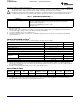
Table 1. ORDERING INFORMATION
(1) (2)
PRODUCT V
OUT
TPS780vvvxxx yyy z VVV is the nominal output voltage for V
OUT(HIGH)
and corresponds to V
SET
pin low.
XXX is the nominal output voltage for V
OUT(LOW)
and corresponds to V
SET
pin high.
YYY is the package designator.
Z is the tape and reel quantity (R = 3000, T = 250).
Adjustable version
(3) (4)
(1) For the most current package and ordering information see the Package Option Addendum at the end of this document, or see the TI
web site at www.ti.com.
(2) Additional output voltage combinations are available on a quick-turn basis using innovative, factory EPROM programming. Minimum-
order quantities apply; contact your sales representative for details and availability.
(3) To order the adjustable version, use TPS78001YYYZ.
(4) The device is either fixed voltage, dual-level V
OUT
, or adjustable voltage only. Device design does not permit a fixed and adjustable
output simultaneously.
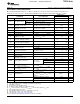
ABSOLUTE MAXIMUM RATINGS
(1)
At T
J
= –40°C to +125°C, unless otherwise noted. All voltages are with respect to GND.
PARAMETER TPS780 Series UNIT
Input voltage range, V
IN
–0.3 to +6.0 V
Enable and V
SET
voltage range, V
EN
and V
VSET
–0.3 to V
IN
+ 0.3
(2)
V
Output voltage range, V
OUT
–0.3 to V
IN
+ 0.3V V
Maximum output current, I
OUT
Internally limited
Output short-circuit duration Indefinite
Total continuous power dissipation, P
DISS
See the Dissipation Ratings table
Human body model (HBM) 2 kV
ESD rating
Charged device model (CDM) 500 V
Operating junction temperature range, T
J
–40 to +125 °C
Storage temperature range, T
STG
–55 to +150 °C
(1) Stresses above these ratings may cause permanent damage. Exposure to absolute maximum conditions for extended periods may
degrade device reliability. These are stress ratings only, and functional operation of the device at these or any other conditions beyond
those specified is not implied.
(2) V
EN
and V
VSET
absolute maximum rating are V
IN
+ 0.3V or +6.0V, whichever is less.
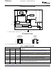
DISSIPATION RATINGS
DERATING FACTOR
BOARD PACKAGE R
θJC
R
θJA
ABOVE T
A
= +25°C T
A
< +25°C T
A
= +70°C T
A
= +85°C
High-K
(1)
DRV 20°C/W 65°C/W 15.4mW/°C 1540mW 845mW 615mW
High-K
(1)
DDC 90°C/W 200°C/W 5.0mW/°C 500mW 275mW 200mW
(1) The JEDEC high-K (2s2p) board used to derive this data was a 3-inch × 3-inch, multilayer board with 1-ounce internal power and
ground planes and 2-ounce copper traces on top and bottom of the board.
2 Submit Documentation Feedback Copyright © 2007–2012, Texas Instruments Incorporated