
Datasheet
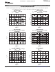

TPS780DRV
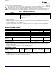
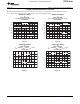
2mmx2mmSON-6
(TOPVIEW)
IN
GND
EN
6
5
4
OUT
N/C
V FB/
SET
1
2
3
Thermal
Pad
(1)
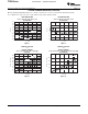
TPS780DDC
TSOT23-5
(TOPVIEW)
OUT
V /FB
SET
IN
GND
EN
1
2
3
5
4
Thermal
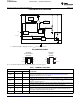
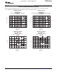
Shutdown
10kW
Current
Limit
Bandgap
IN
EN
OUT
EPROM
MUX
V
SET
/FB
(1)
LOGIC
Active
Pull-
Down
GND
TI Information — Selective Disclosure
TPS780 Series
SBVS083D –JANUARY 2007–REVISED SEPTEMBER 2012
www.ti.com
FUNCTIONAL BLOCK DIAGRAM
(1) Feedback pin (FB) for adjustable versions; V
SET
for fixed voltage versions.
PIN CONFIGURATIONS
(2) It is recommended that the SON package thermal pad be connected to ground.
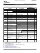
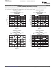
Table 2. TERMINAL FUNCTIONS
TERMINAL
NAME DRV DDC DESCRIPTION
Regulated output voltage pin. A small (1μF) ceramic capacitor is needed from this pin to
OUT 1 5 ground to assure stability. See the Input and Output Capacitor Requirements in the
Application Information section for more details.
N/C 2 — Not connected.
Feedback pin (FB) for adjustable versions; V
SET
for fixed voltage versions. Driving the select
V
SET
/FB 3 4 pin (V
SET
) below 0.4V selects preset output voltage high. Driving the V
SET
pin over 1.2V
selects preset output voltage low.
Driving the enable pin (EN) over 1.2V turns on the regulator. Driving this pin below 0.4V puts
EN 4 3
the regulator into shutdown mode, reducing operating current to 18nA typical.
GND 5 2 Ground pin.
Input pin. A small capacitor is needed from this pin to ground to assure stability. Typical input
IN 6 1 capacitor = 1.0μF. Both input and output capacitor grounds should be tied back to the IC
ground with no significant impedance between them.
Thermal pad Thermal pad — It is recommended that the SON package thermal pad be connected to ground.
4 Submit Documentation Feedback Copyright © 2007–2012, Texas Instruments Incorporated