
Datasheet

TPS78825, TPS78833
SLVS382A – JUNE 2001 – REVISED JULY 2001
3
www.ti.com
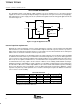
electrical characteristics over recommended operating free-air temperature range EN = 0
,
T
J
= –40 to 125 °C, V
I
= V
O(typ)
+ 1 V, I
O
= 1 mA, C
o
= 4.7 µF, C
(SR)
= 0.01 µF (unless otherwise noted)
PARAMETER TEST CONDITIONS MIN TYP MAX UNIT
V
I
Input voltage (see Note 2) 2.7 10 V
I
O
Continuous output current (see Note 3) 0 150 mA
T
J
Operating junction temperature –40 125 °C
TPS78825
T
J
= 25°C 2.5
Out
p
ut voltage
TPS78825
10 µA< I
O
< 150 mA, 3.5 V < V
I
< 10 V 2.425 2.575
V
Output voltage
TPS78833
T
J
= 25°C 3.3
V
TPS78833
10 µA< I
O
< 150 mA, 3.8 V < V
I
< 10 V 3.201 3.399
Quiescent current (GND current)
10 µA< I
O
< 450 mA, T
J
= 25°C 17
µA
Quiescent current (GND current)
10 µA< I
O
< 150 mA 28
µA
Load regulation 10 µA< I
O
< 200 mA, T
J
= 25°C 12 mV
Output volta
g
e line re
g
ulation (∆V
O
/V
O
)
V
O
+ 1 V < V
I
≤ 10 V, T
J
= 25°C 0.04
%/V
Out ut
voltage
line
regulation
(∆V
O
/V
O
)
(see Note 5)
V
O
+ 1 V < V
I
≤ 10 V 0.1
%/V
Output noise voltage (TPS78833)
BW = 200 Hz to 100 kHz,
I
O
= 150 mA,
T
J
= 25°C,
C
o
= 10 µF,
C
(SR)
= 0.47 µF
56 µV
RMS
R
L
= 22 Ω
,
C
(byp)
= 0.01 µF 10
Time, start-up (TPS78833)
R
L
=
22
Ω
,
C
o
=
10 µF,
C
(byp)
= 0.1 µF 50
ms
Time,
start u
(TPS78833)
C
o
=
10
µF,
T
J
= 25°C
C
(byp)
= 0.47 µF 300
ms
Output current limit
V
O
=
0 V (see Note 4)
350 750 mA
Standby current EN = 0 V, 2.7 V < V
I
< 10 V 1 2 µA
High level enable input voltage 2.7 V < V
I
< 10 V 1.7 V
Low level enable input voltage 2.7 V < V
I
< 10 V 0.9 V
Input current (EN) EN = 0 –1 1 µA
Power supply ripple rejection TPS78833
f = 1 kHz,
T
J
= 25°C,
C
o
= 10 µF
C
(SL)
= 0.01 µF,
I
O
= 150 mA,
70 dB
Dropout voltage (see Note 6)
TPS78833
I
O
= 150 mA, T
J
= 25°C 150
mV
Dropout voltage (see Note 6) TPS78833
I
O
= 150 mA 300
mV
NOTES: 2. To calculate the minimum input voltage for your maximum output current, use the following formula:
V
I
(min) = V
O
(max) + V
DO
(max load)
3. Continuous output current and operating junction temperature are limited by internal protection circuitry, but it is not recommended
that the device operate under conditions beyond those specified in this table for extended periods of time.
4. The minimum IN operating voltage is 2.7 V or V
O(typ)
+ 1 V, whichever is greater. The maximum IN voltage is 5.5 V. The maximum
output current is 200 mA.
5. If V
O
≤ 2.5 V then V
Imin
= 2.7 V, V
Imax
= 5.5 V:
Line regulation (mV) +
ǒ
%ńV
Ǔ
V
O
ǒ
V
Imax
* 2.7 V
Ǔ
100
1000
If V
O
> 2.5 V then V
Imin
= V
O
+ 1 V, V
Imax
= 5.5 V.
6. IN voltage equals V
O
(typ) – 100 mV