
Datasheet
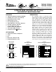
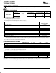
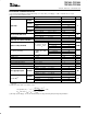
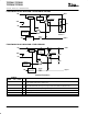
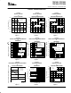
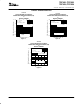
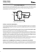
Table Of Contents
- FEATURES
- APPLICATIONS
- DESCRIPTION
- ORDERING INFORMATION
- ABSOLUTE MAXIMUM RATINGS
- PACKAGE DISSIPATION RATING
- RECOMMENDED OPERATING CONDITIONS
- ELECTRICAL CHARACTERISTICS
- FUNCTIONAL BLOCK DIAGRAM—ADJUSTABLE VERSION
- FUNCTIONAL BLOCK DIAGRAM—FIXED VERSION
- Terminal Functions
- TYPICAL CHARACTERISTICS
- APPLICATION INFORMATION
- MECHANICAL DATA
TPS79201, TPS79225
TPS79228, TPS79230
SLVS337B – MARCH 2001 – REVISED MAY 2002
ULTRALOW-NOISE, HIGH PSRR, FAST RF 100-mA
LOW-DROPOUT LINEAR REGULATORS
(3,00 mm x 3,00 mm)
Actual Size
(3,00 mm x 3,00 mm)
Actual Size
FEATURES
D 100-mA Low-Dropout Regulator With EN
D Available in 2.5-V, 2.8-V, 3-V, and Adj.
D High PSRR (75 dB at 10 kHz)
D Ultralow Noise (27 µV)
D Fast Start-Up Time (50 µs)
D Stable With Any 1-µF Ceramic Capacitor
D Excellent Load/Line Transient
D Very Low Dropout Voltage
(55 mV at Full Load, TPS79230)
D 5-Pin SOT23 (DBV) Package
D TPS791xx Provides EN Options
APPLICATIONS
D Cellular and Cordless Telephones
D VCOs
D RF
D Bluetooth, Wireless LAN
D Handheld Organizers, PDA
DESCRIPTION
The TPS792xx family of low-dropout (LDO)
low-power linear voltage regulators features high
power supply rejection ratio (PSRR), ultralow
noise, fast start-up, and excellent line and load
transient responses in a small outline, SOT23,
package. Each device in the family is stable, with
a small 1-µF ceramic capacitor on the output. The
family uses an advanced, proprietary BiCMOS
fabrication process to yield extremely low dropout
voltages (e.g., 55 mV at 100 mA, TPS79230).
Each device achieves fast start-up times
(approximately 50 µs with a 0.001 µF bypass
capacitor) while consuming very low quiescent
current (170 µA typical). Moreover, when the
device is placed in standby mode, the supply
current is reduced to less than 1 µA. The
TPS79228 exhibits approximately 27 µV
RMS
of
output voltage noise with a 0.1 µF bypass
capacitor. Applications with analog components
that are noise sensitive, such as portable RF
electronics, benefit from the high PSRR and low
noise features as well as the fast response time.
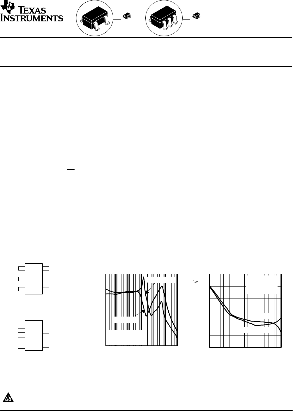
10 100 1 k 10 k
20
50
90
100 k 1 M 10 M
Ripple Rejection – dB
f – Frequency – Hz
TPS79228
RIPPLE REJECTION
vs
FREQUENCY
I
O
= 10 mA
60
0
V
I
= 3.8 V
C
o
= 10 µF
C
(byp)
= 0.01 µF
I
O
= 100 mA
10
30
40
70
80
f – Frequency – Hz
1k 10k 100k
I
O
= 1 mA
V
I
= 3.8 V
C
o
= 1 µF
C
(byp)
= 0.1 µF
100
I
O
= 100 mA
TPS79228
OUTPUT SPECTRAL NOISE DENSITY
vs
FREQUENCY
0
0.05
0.1
0.15
0.2
0.25
0.3
3
2
4
5
DBV PACKAGE
(TOP VIEW)
1IN
GND
EN
OUT
BYPASS
Fixed Option
3
2
4
6
DBV PACKAGE
(TOP VIEW)
1IN
GND
EN
OUT
BYPASS
5
FB
Adjustable Option
V/ HzOutput Spectral Noise Density –
µ
PRODUCTION DATA information is current as of publication date. Products
conform to specifications per the terms of Texas Instruments standard warranty.
Production processing does not necessarily include testing of all parameters.
Please be aware that an important notice concerning availability, standard warranty, and use in critical applications of Texas Instruments
semiconductor products and disclaimers thereto appears at the end of this data sheet.
www.ti.com
Copyright 2002, Texas Instruments Incorporated
Bluetooth is a trademark owned by the Bluetooth SIG, Inc.