
Datasheet


Thermal Guidelines and Layout Recommendations
www.ti.com
5 Thermal Guidelines and Layout Recommendations
Thermal management is a key component of design of any power converter and is especially important
when the power dissipation in the LDO is high. Use the following formula to approximate the maximum
power dissipation for the particular ambient temperature:
T
J
= T
A
+ P
d
x θ
JA
(2)
where:
T
J
is the junction temperature
T
A
is the ambient temperature
P
D
is the power dissipation in the device (Watts)
θ
JA
is the thermal resistance from junction to ambient.
All temperatures are in degrees Celcius. The maximum silicon junction temperature, T
J
, must not be
allowed to exceed 125°C. The layout design must use copper trace and plane areas with care, as thermal
sinks. Do not to allow T
J
to exceed the absolute maximum rating under all temperature conditions and
voltage conditions across the part.
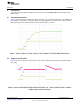
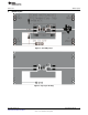
The layout should consider carefully the thermal design of the PCB for optimal performance over
temperature. For this EVM, Figure 5 shows that the DQN package footprint employes a thermal pad for
further cooling the part. The thermal pad contains a single 6.mil thermal via connection to the bottom side
copper ground plane as well as a direct connection to the top side surface copper over the ground pad/pin
for IC. The PCB is a two layer board with 2.oz. copper on top and bottom layers. The DQN package
drawing can be found at the Texas Instruments web site in the product folder for the TPS707 LDO.
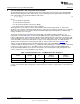
Table 1 repeats information from the Dissipation Ratings Table of the TPS7A4001 data sheet for
comparison with the thermal resistance, θ
JA
, calculated for this EVM layout to show the variation in thermal
resistances for given copper areas. The High-K value is determined using a standard JEDEC high-k
(2s2p) board having dimensions of 3-inch x 3-inch with 1-ounce internal power and ground planes and
2-ounce copper traces on top and bottom of the board.
Table 1. Thermal Resistance, θ
JA
, and Maximum Power Dissipation
Max Dissipation without Max Dissipation without
Board Package θ
JA
Derating Derating
(T
A
= 25°C) (T
A
= 70°C)
High-K DGN 55.1°C/W 1.83W 1.08W
TPS7A4001EVM-709 DGN 49.0°C/W 2.04W 1.12W
The thermal resistance for the TPS7A4001EVM-709, θ
JA
, is the measured value for this particular layout
scheme. The maximum power dissipation is proportional to the volume of copper volume connected to the
package.
4
TPS7A4001EVM-709 SLVU448–March 2011
Submit Documentation Feedback
© 2011, Texas Instruments Incorporated