
Datasheet
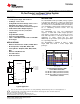
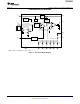


IN
EN
SS
PG
OUT
SNS
C
SS
C
IN
C
OUT
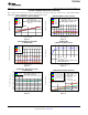
1.5 V
GND
1.2 V = 0.5 V
+ 100 mV
+ 200 mV
+ 400 mV
ref
TPS7A7200
FB
1.6V
800mV400mV200mV
100mV
50mV
Optional
C
FF
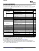
0
1
2
3
4
5
6
1.5V to 1.0V1.5V to 1.2V
1.8V to 1.5V
2.5V to 1.8V
3.0V to 2.5V
3.3V to 3.0V
5.5V to 5.0V
0
1
2
3
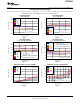
Time (100µs/div)
Output Voltage (V)
Output Current (A)
Output Current
Output Current Slew Rate: 1A/µs
G311
TPS7A7200
www.ti.com
SBVS136E –MARCH 2012–REVISED SEPTEMBER 2013
2-A, Fast-Transient, Low-Dropout Voltage Regulator
Check for Samples: TPS7A7200
1
FEATURES
DESCRIPTION
234
• Low Dropout Voltage: 180 mV at 2 A
The TPS7A7200 low-dropout (LDO) voltage regulator
• V
IN
Range: 1.5 V to 6.5 V
is designed for applications seeking very-low dropout
capability (180 mV at 2 A) with an input voltage from
• Configurable Fixed V
OUT
Range: 0.9 V to 3.5 V
1.5 V to 6.5 V. The TPS7A7200 offers an innovative,
Adjustable V
OUT
Range: 0.9 V to 5.0 V
user-configurable, output-voltage setting from 0.9 V to
• Very Good Load and Line Transient Response
3.5 V, eliminating external resistors and any
• Stable with Ceramic Output Capacitor
associated error.
• 1.5% Accuracy over Line, Load, and
The TPS7A7200 has very fast load-transient
Temperature
response, is stable with ceramic output capacitors,
• Programmable Softstart
and supports a better than 2% accuracy over line,
load, and temperature. A soft-start pin allows for an
• Power Good (PG) Output
application to reduce inrush into the load.
• 3-mm × 3-mm QFN-16 and 5-mm × 5-mm QFN-
Additionally, an open-drain, power-good signal allows
20 Packages
for sequencing power rails.
The TPS7A7200 is available in 3-mm × 3-mm,
APPLICATIONS
16-pin QFN and 5-mm × 5-mm, 20-pin QFN
• Wireless Infrastructure: SerDes, FPGA, DSP™
packages.
• RF Components: VCO, ADC, DAC, LVDS
• Set-Top Boxes: Amplifier, ADC, DAC, FPGA,
DSP
• Wireless LAN, Bluetooth
®
• PCs and Printers
• Audio and Visual
Load Transient Response with
Seven Different Results:
1.5 V
IN
to 1.0 V
OUT
, 1.5 V
IN
to 1.2 V
OUT
,
1.8 V
IN
to 1.5 V
OUT
, 2.5 V
IN
to 1.8 V
OUT
,
3.0 V
IN
to 2.5 V
OUT
, 3.3 V
IN
to 3.0 V
OUT
,
and 5.5 V
IN
to 5.0 V
OUT
Typical Application
1
Please be aware that an important notice concerning availability, standard warranty, and use in critical applications of
Texas Instruments semiconductor products and disclaimers thereto appears at the end of this data sheet.
2DSP is a trademark of Texas Instruments.
3Bluetooth is a registered trademark of Bluetooth SIG, Inc.
4All other trademarks are the property of their respective owners.
PRODUCTION DATA information is current as of publication date.
Copyright © 2012–2013, Texas Instruments Incorporated
Products conform to specifications per the terms of the Texas
Instruments standard warranty. Production processing does not
necessarily include testing of all parameters.