
- TVP5147M1PFP NTSC/PAL/SECAM 2x10-Bit Digital Video Decoder (Rev. A


Functional Description
15
SLES140A—March 2007 TVP5147M1PFP
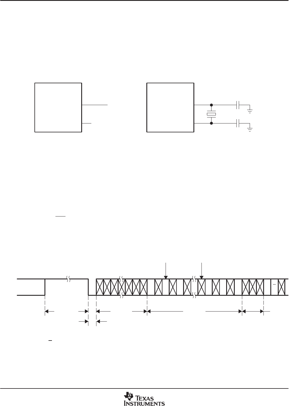
2.3 Clock Circuits
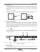
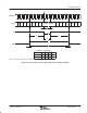
An internal line-locked PLL generates the system and pixel clocks. A 14.318-MHz clock is required to drive
the PLL. This can be input to the TVP5147M1 decoder at the 1.8-V level on terminal 74 (XTAL1), or a crystal
of 14.318-MHz fundamental resonant frequency can be connected across terminals 74 and 75 (XTAL2). If a
parallel resonant circuit is used as shown in Figure 2−10, then the external capacitors must have the following
relationship:
C
L1
= C
L2
= 2C
L
− C
STRAY
,
where C
STRAY
is the terminal capacitance with respect to ground. Figure 2−10 shows the reference clock
configurations. The TVP5147M1 decoder generates the DATACLK signal used for clocking data.
TVP5147M1
74
XTAL1
14.318-MHz
Crystal
75
XTAL2
TVP5147M1
74
XTAL1
75
XTAL2
C
L1
C
L2
14.318-MHz
Clock
Figure 2−10. Reference Clock Configurations
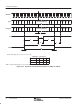
2.4 Real-Time Control (RTC)
Although the TVP5147M1 decoder is a line-locked system, the color burst information is used to determine
accurately the color subcarrier frequency and phase. This ensures proper operation with nonstandard video
signals that do not follow exactly the required frequency multiple between color subcarrier frequency and video
line frequency. The frequency control word of the internal color subcarrier PLL and the subcarrier reset bit are
transmitted via terminal 37 (GLCO) for optional use in an end system (for example, by a video encoder). The
frequency control word is a 23-bit binary number. The instantaneous frequency of the color subcarrier can be
calculated using the following equation:
F
PLL
+
F
ctrl
2
23
F
sclk
where F
PLL
is the frequency of the subcarrier PLL, F
ctrl
is the 23-bit PLL frequency control word, and F
sclk
is
two times the pixel frequency. This information can be generated on the GLCO terminal. Figure 2−11 shows
the detailed timing diagram.
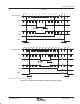
RTC
45 CLK18 CLK
L
S
B
0
3 CLK128 CLK
23-Bit Fsc PLL Increment
Start
Bit
1 CLK
RS
Invalid
Sample
Valid
Sample
M
S
B
22
Reserved
NOTE: RTC reset bit (R) is active-low, Sequence bit (S) PAL: 1 = (R-Y) line normal, 0 = (R-Y) line inverted, NTSC: 1 = no change
Figure 2−11. RTC Timing
2.5 Output Formatter
The output formatter sets how the data is formatted for output on the TVP5147M1 output buses. Table 2−1
shows the available output modes.