
- TVP5147M1PFP NTSC/PAL/SECAM 2x10-Bit Digital Video Decoder (Rev. A

Functional Description
26
SLES140A—March 2007TVP5147M1PFP
2.7.2 VBI Raw Data Output
The TVP5147M1 decoder can output raw A/D video data at twice the sampling rate for external VBI slicing.
This is transmitted as an ancillary data block, although somewhat differently from the way the sliced VBI data
is transmitted in the FIFO format as described in Section 2.7.1. The samples are transmitted during the active
portion of the line. VBI raw data uses ITU-R BT.656 format having only luma data. The chroma samples are
replaced by luma samples. The TVP5147M1 decoder inserts a four-byte preamble 000h 3FFh 3FFh 180h
before data start. There are no checksum bytes and fill bytes in this mode.
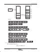
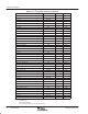
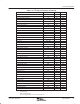
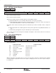
Table 2−8. VBI Raw Data Output Format
BYTE
NO.
D9
(MSB)
D8 D7 D6 D5 D4 D3 D2 D1 D0
(LSB)
DESCRIPTION
0 0 0 0 0 0 0 0 0 0 0
1 1 1 1 1 1 1 1 1 1 1
VBI raw data preamble
2 1 1 1 1 1 1 1 1 1 1
VBI raw data preamble
3 0 1 1 0 0 0 0 0 0 0
4 1. Data
5 2. Data
2 pixel rate luma data
: :
2× pixel rate luma data
(i.e., NTSC 601: n = 1707)
n−1 n−5. Data
(i.e., NTSC 601: n = 1707)
n n–4. Data
2.8 Reset and Initialization
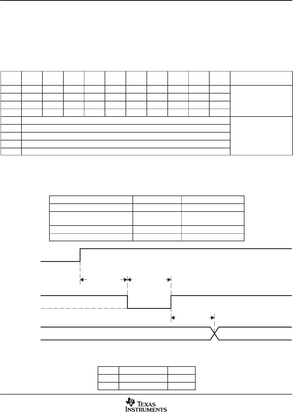
Reset is initiated at power up or any time terminal 34 (RESETB) is brought low. Table 2−9 describes the status
of the TVP5147M1 terminals during and immediately after reset.
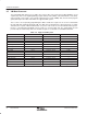
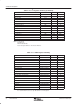
Table 2−9. Reset Sequence
SIGNAL NAME DURING RESET RESET COMPLETED
Y[9:0], C[9:0] Input High-impedance
RESETB, PWDN, SDA, SCL, FSS,
AVID, GLCO, HS, VS, FID
Input Input
INTREQ Input Output
DATACLK Output High-impedance
200 ns (min)
RESETB
(Pin 34)
1 ms (min)
Invalid I
2
C Cycle Valid
Normal Operation
Reset
1 ms (min)
SDA
(Pin 29)
POWER
(3.3 V and 1.8 V)
Figure 2−18. Reset Timing
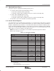
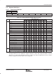
The following register writes must be made before normal operation of the device.
STEP I
2
C SUBADDRESS I
2
C DATA
1 0x03 0x01
2 0x03 0x00