
- TVP5147M1PFP NTSC/PAL/SECAM 2x10-Bit Digital Video Decoder (Rev. A

Functional Description
27
SLES140A—March 2007 TVP5147M1PFP
2.9 Adjusting External Syncs
The proper sequence to program the following external syncs is:
• To set NTSC, PAL-M, NTSC 443, PAL60 (525-line modes):
− Set the video standard to NTSC (register 02h)
− Set HSYNC, VSYNC, VBLK, and AVID external syncs (registers 16h through 24h)
• To set PAL, PAL-N, SECAM (625-line modes):
− Set the video standard to PAL (register 02h)
− Set HSYNC, VSYNC, VBLK, and AVID external syncs (registers 16h through 24h)
• For autoswitch, set the video standard to autoswitch (register 02h)
2.10 Internal Control Registers
The TVP5147M1 decoder is initialized and controlled by a set of internal registers that define the operating
parameters of the entire device. Communication between the external controller and the TVP5147M1 is
through a standard I
2
C host port interface, as described earlier. Table 2−10 shows the summary of these
registers. Detailed programming information for each register is described in the following sections. Additional
registers are accessible through an indirect procedure involving access to an internal 24-bit address wide
VBUS. Table 2−11 shows the summary of the VBUS registers.
NOTE: Do not write to reserved registers. Reserved bits in any defined register must be written
with 0s, unless otherwise noted.
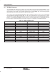
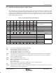
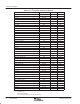
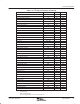
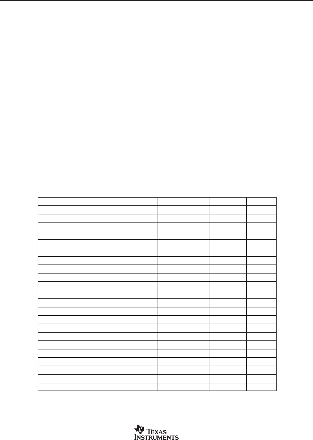
Table 2−10. I
2
C Register Summary
REGISTER NAME I
2
C SUBADDRESS DEFAULT R/W
Input select 00h 00h R/W
AFE gain control 01h 0Fh R/W
Video standard 02h 00h R/W
Operation mode 03h 00h R/W
Autoswitch mask 04h 23h R/W
Color killer 05h 10h R/W
Luminance processing control 1 06h 00h R/W
Luminance processing control 2 07h 00h R/W
Luminance processing control 3 08h 02h R/W
Luminance brightness 09h 80h R/W
Luminance contrast 0Ah 80h R/W
Chrominance saturation 0Bh 80h R/W
Chroma hue 0Ch 00h R/W
Chrominance processing control 1 0Dh 00h R/W
Chrominance processing control 2 0Eh 0Eh R/W
Reserved 0Fh−15h
AVID start pixel 16h−17h 055h R/W
AVID stop pixel 18h−19h 325h R/W
HSYNC start pixel 1Ah−1Bh 000h R/W
HSYNC stop pixel 1Ch−1Dh 040h R/W
VSYNC start line 1Eh−1Fh 004h R/W
VSYNC stop line 20h−21h 007h R/W
NOTE: R = Read only
W = Write only
R/W = Read and write
Reserved register addresses must not be written to.