
Datasheet
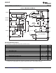
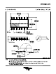
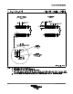

RT
VREF
NI
INV
COMP
STATUS
+VIN
CT
EXTCLK
N/C
DRIVERB
DRIVERA
GND
N/C
DPACKAGE
(TOP VIEW)
N/C = No internal connection
UC2901-EP
www.ti.com
SLUS709A –DECEMBER 2006–REVISED MARCH 2010
ISOLATED FEEDBACK GENERATOR
Check for Samples: UC2901-EP
1
FEATURES
• Controlled Baseline • Internal Carrier Oscillator Usable to 5 MHz
– One Assembly/Test Site, One Fabrication • Modulator Synchronizable to an External
Site Clock
• Extended Temperature Performance of –55°C • Loop Status Monitor
to 125°C
• Enhanced Diminishing Manufacturing Sources
(DMS) Support
• Enhanced Product-Change Notification
• Qualification Pedigree
(1)
• Amplitude-Modulation System for Transformer
Coupling an Isolated Feedback Error Signal
• Low-Cost Alternative to Optical Couplers
• Internal 1% Reference and Error Amplifier
(1) Component qualification in accordance with JEDEC and
industry standards to ensure reliable operation over an
extended temperature range. This includes, but is not limited
to, Highly Accelerated Stress Test (HAST) or biased 85/85,
temperature cycle, autoclave or unbiased HAST,
electromigration, bond intermetallic life, and mold compound
life. Such qualification testing should not be viewed as
XXX
justifying use of this component beyond specified
performance and environmental limits.
DESCRIPTION
The UC2901 is designed to solve many of the problems associated with closing a feedback control loop across a
voltage isolation boundary. As a stable and reliable alternative to an optical coupler, UC2901 features an
amplitude modulation system that allows a loop error signal to be coupled with a small RF transformer or
capacitor.
The programmable, high-frequency oscillator within the UC2901 permits the use of smaller, less-expensive
transformers, which can readily be built to meet the isolation requirements of today's line-operated power
systems. As an alternative to RF operation, the external clock input to these devices allows synchronization to a
system clock or to the switching frequency of an SMPS.
An additional feature is a status monitoring circuit that provides an active low output when the sensed error
voltage is within ±10% of the reference. The DRIVERA output, DRIVERB output, and STATUS output are
disabled until the input supply has reached a sufficient level to allow proper operation of the device.
Because these devices also can be used as a DC driver for optical couplers, the benefits of 4.5 V to 40 V supply
operation, a 1% accurate reference, and a high-gain general-purpose amplifier offer advantages, even though an
AC system may not be desired.
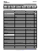
ORDERING INFORMATION
T
A
PACKAGE
(1)
ORDERABLE PART NUMBER TOP-SIDE MARKING
–55°C to 125°C D (SOIC) UC2901MDREP UC2901MEP
(1) Package drawings, standard packing quantities, thermal data, symbolization, and PCB design guidelines are available at
www.ti.com/sc/package.
1
Please be aware that an important notice concerning availability, standard warranty, and use in critical applications of Texas
Instruments semiconductor products and disclaimers thereto appears at the end of this data sheet.
PRODUCTION DATA information is current as of publication date.
Copyright © 2006–2010, Texas Instruments Incorporated
Products conform to specifications per the terms of the Texas
Instruments standard warranty. Production processing does not
necessarily include testing of all parameters.