
Datasheet

UC1572
UC2572
UC3572
DESCRIPTION
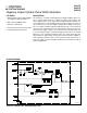
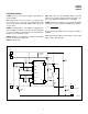
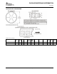
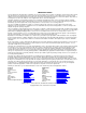
The UC3572 is a negative output flyback pulse width modulator which con
-
verts a positive input voltage to a regulated negative output voltage. The
chip is optimized for use in a single inductor negative flyback switching con
-
verter employing an external PMOS switch. The block diagram consists of
a precision reference, an error amplifier configured for voltage mode opera
-
tion, an oscillator, a PWM comparator with latching logic, and a 0.5A peak
gate driver. The UC3572 includes an undervoltage lockout circuit to insure
sufficient input supply voltage is present before any switching activity can
occur, and a pulse-by-pulse current limit. Output current can be sensed and
limited to a user determined maximum value. The UVLO circuit turns the
chip off when the input voltage is below the UVLO threshold. In addition, a
sleep comparator interfaces to the UVLO circuit to turn the chip off. This re
-
duces the supply current to only 50µA, making the UC3572 ideal for battery
powered applications.
Negative Output Flyback Pulse Width Modulator
FEATURES
•
Simple Single Inductor Flyback PWM
for Negative Voltage Generation
•
Drives External PMOS Switch
•
Contains UVLO Circuit
•
Includes Pulse-by-Pulse Current Limit
•
Low 50µA Sleep Mode Current
SLUS275A - MARCH 1999 - REVISED AUGUST 2001
BLOCK DIAGRAM
UDG-94094-2