
Datasheet


UC1610
UC3610
SLUS339B − JUNE 1993 − REVISED DECEMBER 2004
2
www.ti.com
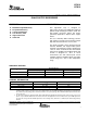
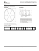
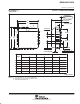
N OR J PACKAGE
TOP VIEW
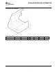
DW PACKAGE
TOP VIEW
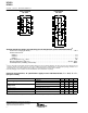
absolute maximum ratings over operating free-air temperature (unless otherwise noted)
†
}
Peak inverse voltage (per diode) 50 V. . . . . . . . . . . . . . . . . . . . . . . . . . . . . . . . . . . . . . . . . . . . . . . . . . . . . . . . . . . . .
Peak forward current
UC1611 1 A. . . . . . . . . . . . . . . . . . . . . . . . . . . . . . . . . . . . . . . . . . . . . . . . . . . . . . . . . . . . . . . . . . . . . . . . . . . . . . . . .
UC2610 1 A. . . . . . . . . . . . . . . . . . . . . . . . . . . . . . . . . . . . . . . . . . . . . . . . . . . . . . . . . . . . . . . . . . . . . . . . . . . . . . . . .
UC3611 3 A. . . . . . . . . . . . . . . . . . . . . . . . . . . . . . . . . . . . . . . . . . . . . . . . . . . . . . . . . . . . . . . . . . . . . . . . . . . . . . . . .
Power dissipation at T
A
= 70°C 1 W. . . . . . . . . . . . . . . . . . . . . . . . . . . . . . . . . . . . . . . . . . . . . . . . . . . . . . . . . . . . . . .
Storage temperature range, T
stg
−65°C to 150°C. . . . . . . . . . . . . . . . . . . . . . . . . . . . . . . . . . . . . . . . . . . . . . . . . . . .
Lead temperature (soldering, 10 seconds) 300°C. . . . . . . . . . . . . . . . . . . . . . . . . . . . . . . . . . . . . . . . . . . . . . . . . . .
†
Stresses beyond those listed under “absolute maximum ratings” may cause permanent damage to the device. These are stress ratings only, and
functional operation of the device at these or any other conditions beyond those indicated under “recommended operating conditions” is not
implied. Exposure to absolute-maximum-rated conditions for extended periods may affect device reliability.
‡
Consult packaging section of databook for thermal limitations and considerations of package.
electrical characteristics, all specifications apply to each individual diode, T
J
= 25°C, T
A
= T
J
,
(except as noted)
PARAMETER TEST CONDITIONS MIN TYP MAX UNITS
Forward voltage drop
I
F
= 100 mA 0.35 0.5 0.7 V
Forward voltage drop
I
F
= 1 A 0.8 1.0 1.3 V
Leakage current
V
R
= 40 V 0.01 0.1 mA
Leakage current
V
R
= 40 V, T
J
= 100°C 0.1 1.0 mA
Reverse recovery 0.5 A forward to 0.5 A reverse 15 ns
Forward recovery 1 A forward to 1.1 V recovery 30 ns
Junction capacitance V
R
= 5 V 70 pF
NOTE: At forward currents of greater than 1.0 A, a parasitic current of approximately 10 mA may be collected by adjacent diodes.
PRODUCT PREVIEW information concerns products in the formative or
design phase of development. Characteristic data and other
specifications are design goals. Texas Instruments reserves the right to
change or discontinue these products without notice.