User’s Guide August 2002 PMP SLUU127
IMPORTANT NOTICE Texas Instruments Incorporated and its subsidiaries (TI) reserve the right to make corrections, modifications, enhancements, improvements, and other changes to its products and services at any time and to discontinue any product or service without notice. Customers should obtain the latest relevant information before placing orders and should verify that such information is current and complete.
EVM IMPORTANT NOTICE Texas Instruments (TI) provides the enclosed product(s) under the following conditions: This evaluation kit being sold by TI is intended for use for ENGINEERING DEVELOPMENT OR EVALUATION PURPOSES ONLY and is not considered by TI to be fit for commercial use.
EVM WARNINGS AND RESTRICTIONS It is important to operate this EVM within the input voltage range of 1.7 V minimum to 7.5 V maximum, bias voltage range of 3.4 V minimum to 7.5 V maximum, and output current of 5 A maximum. Exceeding the specified input range may cause unexpected operation and/or irreversible damage to the EVM. If there are questions concerning the input range, please contact a TI field representative prior to connecting the input power.
Related Documentation From Texas Instruments Preface About This Manual This user’s guide describes the characteristics, operation and use of the UC385EVM-207 High-Current, Low-Input Voltage, Low-Dropout Linear Regulator evaluation module (EVM). The user’s guide includes a schematic diagram, printed circuit board (PCB) layouts, and bill of materials. Electronic PCB layout files are available upon request.
iv
Contents 1 Introduction . . . . . . . . . . . . . . . . . . . . . . . . . . . . . . . . . . . . . . . . . . . . . . . . . . . . . . . . . . . . . . . . . . . . . 1.1 Background . . . . . . . . . . . . . . . . . . . . . . . . . . . . . . . . . . . . . . . . . . . . . . . . . . . . . . . . . . . . . . . . 1.2 Performance Specification Summary . . . . . . . . . . . . . . . . . . . . . . . . . . . . . . . . . . . . . . . . . . 1.3 Modifications . . . . . . . . . . . . . . . . . . . . . . . . . . . . . .
Contents 2–1 2–2 2–3 2–4 2–5 3–1 3–2 3–3 3–4 4–1 Test Setup . . . . . . . . . . . . . . . . . . . . . . . . . . . . . . . . . . . . . . . . . . . . . . . . . . . . . . . . . . . . . . . . . . . Power up . . . . . . . . . . . . . . . . . . . . . . . . . . . . . . . . . . . . . . . . . . . . . . . . . . . . . . . . . . . . . . . . . . . . Line Transient Response . . . . . . . . . . . . . . . . . . . . . . . . . . . . . . . . . . . . . . . . . . . . . . . . . . . . . . . Load Transient Response . . . .
Chapter 1 This chapter contains background information for the UCx82-x and UCx85-x regulators and support documentation for the UC385EVM-207 evaluation module. The EVM performance specifications are also given. Topic Page 1.1 Background . . . . . . . . . . . . . . . . . . . . . . . . . . . . . . . . . . . . . . . . . . . . . . . . . . 1-2 1.2 Performance Specification Summary . . . . . . . . . . . . . . . . . . . . . . . . . . . 1-2 1.3 Modifications . . . . . . . . . . . . . . . . . .
Background 1.1 Background The purpose of the UC385EVM-207 is to facilitate evaluation of the UCx82-x and UCx85-x families of devices. The UC385EVM consists of the SLVP207 PCB, one UC385-ADJ adjustable, 5-A linear regulator in a TO-263 package, and supporting passive components. The adjustable device has been configured to output 1.2 V using a feedback resistor. The SLVP207 PCB is designed to accommodate multiple devices with similar pin-outs in different packages (i.e., TO–220, TO–263, or SOT–223).
Modifications 1.3 Modifications The UC385EVM-207 is designed to allow parts to be easily interchanged. Although the EVM is designed with a UC385-ADJ regulator in a TO-263 package, the SLVP207 EVM board can also accommodate any other member of the UCx82 or UCx85 families in either the TO-263 or TO-220 or any device with the same pinout in a TO-220, TO-263, or SOT-223 package. Passive elements such as the output capacitors (C4, C5) and the input capacitor (C3) can be easily changed.
1-4
Chapter 2 This chapter describes how to properly connect, setup, and use the UC385EVM-207. It also presents the test results for the more common tests performed using the EVM. Topic Page 2.1 Test Setup for DC Testing . . . . . . . . . . . . . . . . . . . . . . . . . . . . . . . . . . . . . . 2-2 2.2 Test Results . . . . . . . . . . . . . . . . . . . . . . . . . . . . . . . . . . . . . . . . . . . . . . . . . .
Test Setup for DC Testing 2.1 Test Setup for DC Testing Figure 2–1.
Test Results 2.2 Test Results Figure 2–2. Power Up Channel 1 is the input voltage and it ramps to 3.3 V. Channel 2 is the output voltage. The bias voltage is 5 V and the output current is 2.5 A. Figure 2–3. Line Transient Response Channel 1 is the input voltage stepped from 1.8 V to 2.8 V. Channel 2 is the output voltage with a dc offset of 1.2 V. The input bias voltage is 5.0 V. The output current is 5 A.
Test Results Figure 2–4. Load Transient Response Channel 2 is the output voltage with a dc offset of 2 V and channel 4 is the output current. The input bias voltage is 5.0 V and the input voltage is 1.8 V. Figure 2–5. PSRR The bias voltage is 5 V. The input voltage is 1.8 V and the output voltage is 1.2 V. The output current is 5 A.
Chapter 3 This chapter provides a description of the SLVP207 board layout and layer illustrations used in the UC385EVM–207. Topic 3.1 Page Layout . . . . . . . . . . . . . . . . . . . . . . . . . . . . . . . . . . . . . . . . . . . . . . . . . . . . . . .
Layout 3.1 Layout The EVM PCB consists of two layers of 1.5 oz. copper. The top side (component) layout of the EVM is shown in Figure 3–1. Large power and ground planes are used to minimize trace resistance. The input capacitor (C3) is located close to the input pin. Proper board layout is critical to ensure the best noise and PSRR performance. The ground side of the output capacitor (C4) is close to the board ground connection for improved transient response.
Layout Figure 3–2. Bottom Side Assembly Figure 3–3.
Layout Figure 3–4.
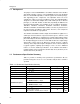
Chapter 4 The EVM schematic and bill of materials are presented in this chapter. Topic Page 4.1 Schematic . . . . . . . . . . . . . . . . . . . . . . . . . . . . . . . . . . . . . . . . . . . . . . . . . . . . 4-2 4.2 Bill of Materials . . . . . . . . . . . . . . . . . . . . . . . . . . . . . . . . . . . . . . . . . . . . . . .
Schematic 4.1 Schematic Figure 4–1. Schematic R2 R5 100 Ω U1 UC385–ADJ JP1 1 R1 J1 1 2 VIN VBIAS GND 1 C3 2 1 µF 3 3 VBIAS GND IN ADJ GND OUT + 4.7 µF 5 0Ω J4 C4 TP2 GND 1 + C5 100 µF + C6 1 R4 1 VOUT FB GND C7 1 J3 1 2 1 TP3 VOUT C2 100 µF J6 3 4 R3 TP1 VIN C1 1 6 J5 Open 4.2 Bill of Materials Table 4–1.